

Redis的内存分析(set/get命令集)

为了知道Redis是如何使用内存的,我分析了源码。这篇文章针对的是set/get命令集,也就是key、value都是简单的字符串。除此之外,Redis还支持像hset/hget命令,它们的value是一个字典,留到以后分析。 首先来看看Redis存储数据的关键数据结构: 1. zmalloc (
为了知道Redis是如何使用内存的,我分析了源码。这篇文章针对的是set/get命令集,也就是key、value都是简单的字符串。除此之外,Redis还支持像hset/hget命令,它们的value是一个字典,留到以后分析。
首先来看看Redis存储数据的关键数据结构:
1. zmalloc (见zmalloc.h)
Redis是用zmalloc管理内存的,其底层可以是glibc malloc、jemalloc、tcmalloc,具体由用户选择,目前的版本默认为jemalloc。本文不分析jemalloc,而是从zmalloc这一层开始往上分析。
zmalloc封装了底层内存管理,并为每一段申请的内存增加了一个头部,大小为PREFIX_SIZE = 8字节,这个头部记录了申请内存的大小。因此每一块申请的内存有额外的8字节内存开销。
2. sds (见sds.h)
sds是Redis使用的字符串工具,取代string.h。sds的结构体如下,包含4=4=8字节的头部,buf后面就是字符串的空间。因此每个字符串需要8字节的额外空间。
struct sdshdr {
unsigned int len;
unsigned int free;
char buf[];
};
3. 哈希表(见dict.h)
这是核心数据结构,所有的key value都存在哈希表内。dict是哈希表的元数据,ht[2]数组是实际的哈希表,ht[0]是当前使用的哈希表;当数据太多(超过了ht[0]的数组大小),就分配2倍大的ht[1],然后逐渐将数据从ht[0]迁移到ht[1]。由于dict结构体是唯一的,它的内存开销可以忽略不计。
dictht是实际的哈希表,包含一个指针数组,数组的每一项是指向dictEntry的指针,被哈希到同一项的数据以链表的方式解决冲突。
typedef struct dict {
dictType *type;
void *privdata;
dictht ht[2];
long rehashidx; /* rehashing not in progress if rehashidx == -1 */
int iterators; /* number of iterators currently running */
} dict;
/* This is our hash table structure. Every dictionary has two of this as we
* implement incremental rehashing, for the old to the new table. */
typedef struct dictht {
dictEntry **table;
unsigned long size;
unsigned long sizemask;
unsigned long used;
} dictht;
typedef struct dictEntry {
void *key;
union {
void *val;
uint64_t u64;
int64_t s64;
double d;
} v;
struct dictEntry *next;
} dictEntry;
在redis中,key是sds字符串,而value则是robj数据结构。当插入一对key-value,会产生一个dictEntry,key指向一个sds字符串,而v.val指向一个robj。dictEntry的大小为24字节。
4. 对象robj(见redis.h)
robj结构体如下。ptr指向数据;type指明数据的类型(比如可以是sds字符串);encoding表示是否进行了编码(即压缩字符串,见下文);lru用于实现lru替换策略,每次查询都会更新lru的值;refcount是引用次数,因为Redis允许共享对象,节约内存。robj结构体的大小为16字节。
#define REDIS_LRU_CLOCK_RESOLUTION 1000 /* LRU clock resolution in ms */
typedef struct redisObject {
unsigned type:4;
unsigned encoding:4;
unsigned lru:REDIS_LRU_BITS; /* lru time (relative to server.lruclock) */
int refcount;
void *ptr;
} robj;
内存分析
每一对key-value,需要一个sds字符串存储key,这需要额外8字节zmalloc头部+8字节sds头部,一共16字节;需要一个robj存储value,robj->ptr实际指向一个sds字符串(假设没有压缩),这需要额外16字节的robj + 8字节zmalloc头部,以及robj->ptr指向的字符串的8字节zmalloc头部和8字节sds头部,一共40字节。
插入哈希表后,需要一个24字节的dictEntry和8字节的zmalloc头部,以及一个指针数组中的8字节指针,一共40字节。
最终,每个key-value对,除去数据本身,一共需要额外 16 +40 +40 = 96字节的元数据。并且这96个字节分属于四个不同的内存区块(这里忽略哈希表指针数组):
- 存储key的sds字符串(8+8+keylen);
- 存储robj(8+16);
- 存储robj->ptr对应的value(8+8+vallen);
- 存储dictEntry(8+24)。
其中2、4是定长的小内存,1、3是变长内存。
对于key-value较小的负载,这些元数据开销并不低;以我上篇实验为例,采用了20字节的key和100字节的value,元数据开销占96/(120+96)=44.4%。
以上为set/get命令的分析,hset/hget命令的内存开销应该会更高,留待以后分析。
Redis如何节约内存
Redis通过对字符串压缩、共享对象等方式节约内存:对于每一个字符串value,Redis都尝试一下方法:
1. 如果字符串全部由数字组成,则尝试将其表示为长整形。最多可以将21字节压缩成8字节。因为指针ptr是8字节,数值可以直接存在ptr里面而无需额外内存,又节约了8字节。
2. 如果整型编码成功,且数值在1-10000之间,则使用共享对象,因为1-10000这些对象已经实现创建好了。
3. 如果整型编码不行,但是字符串又
原文地址:Redis的内存分析(set/get命令集), 感谢原作者分享。

Hot AI Tools

Undresser.AI Undress
AI-powered app for creating realistic nude photos

AI Clothes Remover
Online AI tool for removing clothes from photos.

Undress AI Tool
Undress images for free

Clothoff.io
AI clothes remover

AI Hentai Generator
Generate AI Hentai for free.

Hot Article
Hot Tools

Notepad++7.3.1
Easy-to-use and free code editor

SublimeText3 Chinese version
Chinese version, very easy to use

Zend Studio 13.0.1
Powerful PHP integrated development environment

Dreamweaver CS6
Visual web development tools

SublimeText3 Mac version
God-level code editing software (SublimeText3)
Hot Topics
 1371
1371
 52
52

 Large memory optimization, what should I do if the computer upgrades to 16g/32g memory speed and there is no change?
Jun 18, 2024 pm 06:51 PM
Large memory optimization, what should I do if the computer upgrades to 16g/32g memory speed and there is no change?
Jun 18, 2024 pm 06:51 PM
For mechanical hard drives or SATA solid-state drives, you will feel the increase in software running speed. If it is an NVME hard drive, you may not feel it. 1. Import the registry into the desktop and create a new text document, copy and paste the following content, save it as 1.reg, then right-click to merge and restart the computer. WindowsRegistryEditorVersion5.00[HKEY_LOCAL_MACHINE\SYSTEM\CurrentControlSet\Control\SessionManager\MemoryManagement]"DisablePagingExecutive"=d
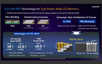 Sources say Samsung Electronics and SK Hynix will commercialize stacked mobile memory after 2026
Sep 03, 2024 pm 02:15 PM
Sources say Samsung Electronics and SK Hynix will commercialize stacked mobile memory after 2026
Sep 03, 2024 pm 02:15 PM
According to news from this website on September 3, Korean media etnews reported yesterday (local time) that Samsung Electronics and SK Hynix’s “HBM-like” stacked structure mobile memory products will be commercialized after 2026. Sources said that the two Korean memory giants regard stacked mobile memory as an important source of future revenue and plan to expand "HBM-like memory" to smartphones, tablets and laptops to provide power for end-side AI. According to previous reports on this site, Samsung Electronics’ product is called LPWide I/O memory, and SK Hynix calls this technology VFO. The two companies have used roughly the same technical route, which is to combine fan-out packaging and vertical channels. Samsung Electronics’ LPWide I/O memory has a bit width of 512
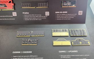 Kingbang launches new DDR5 8600 memory, offering CAMM2, LPCAMM2 and regular models to choose from
Jun 08, 2024 pm 01:35 PM
Kingbang launches new DDR5 8600 memory, offering CAMM2, LPCAMM2 and regular models to choose from
Jun 08, 2024 pm 01:35 PM
According to news from this site on June 7, GEIL launched its latest DDR5 solution at the 2024 Taipei International Computer Show, and provided SO-DIMM, CUDIMM, CSODIMM, CAMM2 and LPCAMM2 versions to choose from. ▲Picture source: Wccftech As shown in the picture, the CAMM2/LPCAMM2 memory exhibited by Jinbang adopts a very compact design, can provide a maximum capacity of 128GB, and a speed of up to 8533MT/s. Some of these products can even be stable on the AMDAM5 platform Overclocked to 9000MT/s without any auxiliary cooling. According to reports, Jinbang’s 2024 Polaris RGBDDR5 series memory can provide up to 8400
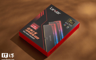 Lexar God of War Wings ARES RGB DDR5 8000 Memory Picture Gallery: Colorful White Wings supports RGB
Jun 25, 2024 pm 01:51 PM
Lexar God of War Wings ARES RGB DDR5 8000 Memory Picture Gallery: Colorful White Wings supports RGB
Jun 25, 2024 pm 01:51 PM
When the prices of ultra-high-frequency flagship memories such as 7600MT/s and 8000MT/s are generally high, Lexar has taken action. They have launched a new memory series called Ares Wings ARES RGB DDR5, with 7600 C36 and 8000 C38 is available in two specifications. The 16GB*2 sets are priced at 1,299 yuan and 1,499 yuan respectively, which is very cost-effective. This site has obtained the 8000 C38 version of Wings of War, and will bring you its unboxing pictures. The packaging of Lexar Wings ARES RGB DDR5 memory is well designed, using eye-catching black and red color schemes with colorful printing. There is an exclusive &quo in the upper left corner of the packaging.
 DDR5 MRDIMM and LPDDR6 CAMM memory specifications are ready for launch, JEDEC releases key technical details
Jul 23, 2024 pm 02:25 PM
DDR5 MRDIMM and LPDDR6 CAMM memory specifications are ready for launch, JEDEC releases key technical details
Jul 23, 2024 pm 02:25 PM
According to news from this website on July 23, the JEDEC Solid State Technology Association, the microelectronics standard setter, announced on the 22nd local time that the DDR5MRDIMM and LPDDR6CAMM memory technical specifications will be officially launched soon, and introduced the key details of these two memories. The "MR" in DDR5MRDIMM stands for MultiplexedRank, which means that the memory supports two or more Ranks and can combine and transmit multiple data signals on a single channel without additional physical The connection can effectively increase the bandwidth. JEDEC has planned multiple generations of DDR5MRDIMM memory, with the goal of eventually increasing its bandwidth to 12.8Gbps, compared with the current 6.4Gbps of DDR5RDIMM memory.
 Longsys displays FORESEE LPCAMM2 notebook memory: up to 64GB, 7500MT/s
Jun 05, 2024 pm 02:22 PM
Longsys displays FORESEE LPCAMM2 notebook memory: up to 64GB, 7500MT/s
Jun 05, 2024 pm 02:22 PM
According to news from this website on May 16, Longsys, the parent company of the Lexar brand, announced that it will demonstrate a new form of memory - FORESEELPCAMM2 at CFMS2024. FORESEELPCAMM2 is equipped with LPDDR5/5x particles, is compatible with 315ball and 496ball designs, supports frequencies of 7500MT/s and above, and has product capacity options of 16GB, 32GB, and 64GB. In terms of product technology, FORESEELPCAMM2 adopts a new design architecture to directly package 4 x32LPDDR5/5x memory particles on the compression connector, realizing a 128-bit memory bus on a single memory module, providing a more efficient packaging than standard memory modules.
 It is reported that Samsung Electronics has confirmed investment in the 1cnm DRAM memory production line of Pyeongtaek P4 factory and aims to put it into operation in June next year.
Aug 12, 2024 pm 04:31 PM
It is reported that Samsung Electronics has confirmed investment in the 1cnm DRAM memory production line of Pyeongtaek P4 factory and aims to put it into operation in June next year.
Aug 12, 2024 pm 04:31 PM
According to news from this site on August 12, Korean media ETNews reported that Samsung Electronics has internally confirmed its investment plan to build a 1cnm DRAM memory production line at the Pyeongtaek P4 factory. The production line is targeted to be put into operation in June next year. Pyeongtaek P4 is a comprehensive semiconductor production center divided into four phases. In the earlier planning, the first phase was for NAND flash memory, the second phase was for logic foundry, and the third and fourth phases were for DRAM memory. Samsung has introduced DRAM production equipment in the first phase of P4, but has shelved the second phase of construction. 1cnm DRAM is the sixth-generation 20~10nm memory process, and each company's 1cnm (or corresponding 1γnm) products have not yet been officially released. Korean media reported that Samsung Electronics plans to start 1cnm memory production at the end of this year. ▲Samsung Pyeongtaek
 It is reported that Samsung Electronics has established a 1dnm DRAM memory technology development team in advance to rebuild its advantages.
May 09, 2024 pm 06:31 PM
It is reported that Samsung Electronics has established a 1dnm DRAM memory technology development team in advance to rebuild its advantages.
May 09, 2024 pm 06:31 PM
According to news from this site on May 9, Korean media Sedaily quoted industry sources as saying that Samsung Electronics recently decided to form a technology development team for 1dnm DRAM memory. At present, the latest process in the DRAM memory industry is the fifth-generation process of the 10+nm series, namely 1bnm; the next-generation DRAM process 1cnm of the three major memory manufacturers - Samsung Electronics, SK Hynix and Micron will be put into use from the third quarter of this year to next year. production; and the 1dnm process is after 1cnm, and mass production is expected to be later than 2026. When Samsung Electronics develops each generation of DRAM technology, it usually does not form a team including semiconductor and process engineers until the PA (Process Architecture) stage close to mass production.
