 Technology peripherals
 It Industry
 Intel explains in detail the Intel 3 process: applying more EUV lithography, increasing the frequency of the same power consumption by up to 18%
Intel explains in detail the Intel 3 process: applying more EUV lithography, increasing the frequency of the same power consumption by up to 18%
According to news from this site on June 19, as part of the 2024 IEEE VLSI seminar activities, Intel recently introduced the technical details of the Intel 3 process node on its official website.
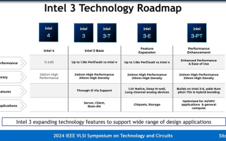
Intel's latest generation of FinFET transistor technology is Intel's latest generation of FinFET transistor technology. Compared with Intel 4, it has added steps to use EUV. It will also be a node family that provides foundry services for a long time, including basic Intel 3 and three variant nodes.

Among them, Intel 3-E natively supports 1.2V high voltage, which is suitable for the manufacturing of analog modules; and the future Intel 3-PT will further improve overall performance and supports finer 9μm pitch TSV and hybrid bonding.
Intel claims that as its "ultimate FinFET process", Intel 3-PT will become the mainstream choice for many years to come, and will be used by internal and external foundry customers together with angstrom-level process nodes.
Compared with Intel3, which only contains 240nm high-performance libraries (note on this site: HP libraries), the Intel4 process introduces the 210nm high-density (HD) library, providing more possibilities in transistor performance orientation.

Intel stated that its basic Intel 3 process can be improved at most compared to the Intel 4 process when using high-density libraries 18% frequency.
In addition, Intel also claimed thatthe basic version of Intel 3 process density has also increased by 10%, achieving a "full node" level improvement.

Intel 3 also provides 12+ in addition to the 14+2 layer of Intel 4 Two new options, 2 and 19+2, are targeted at low-cost and high-performance applications respectively.

The above is the detailed content of Intel explains in detail the Intel 3 process: applying more EUV lithography, increasing the frequency of the same power consumption by up to 18%. For more information, please follow other related articles on the PHP Chinese website!

Hot AI Tools

Undresser.AI Undress
AI-powered app for creating realistic nude photos

AI Clothes Remover
Online AI tool for removing clothes from photos.

Undress AI Tool
Undress images for free

Clothoff.io
AI clothes remover

Video Face Swap
Swap faces in any video effortlessly with our completely free AI face swap tool!

Hot Article

Hot Tools

Notepad++7.3.1
Easy-to-use and free code editor

SublimeText3 Chinese version
Chinese version, very easy to use

Zend Studio 13.0.1
Powerful PHP integrated development environment

Dreamweaver CS6
Visual web development tools

SublimeText3 Mac version
God-level code editing software (SublimeText3)

Hot Topics
 1666
1666
 14
14
 1425
1425
 52
52
 1328
1328
 25
25
 1273
1273
 29
29
 1253
1253
 24
24
 Intel announces Wi-Fi 7 BE201 network card, supports CNVio3 interface
Jun 07, 2024 pm 03:34 PM
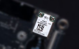
According to news from this site on June 1, Intel updated the support document on May 27 and announced the product details of the Wi-Fi7 (802.11be) BE201 network card code-named "Fillmore Peak2". Source of the above picture: benchlife website Note: Unlike the existing BE200 and BE202 which use PCIe/USB interface, BE201 supports the latest CNVio3 interface. The main specifications of the BE201 network card are similar to those of the BE200. It supports 2x2TX/RX streams, supports 2.4GHz, 5GHz and 6GHz. The maximum network speed can reach 5Gbps, which is far lower than the maximum standard rate of 40Gbit/s. BE201 also supports Bluetooth 5.4 and Bluetooth LE.
 Intel Core Ultra 9 285K processor exposed: CineBench R23 multi-core running score is 18% higher than i9-14900K
Jul 25, 2024 pm 12:25 PM
According to news from this website on July 25, the source Jaykihn posted a tweet on the X platform yesterday (July 24), sharing the running score data of the Intel Core Ultra9285K "ArrowLake-S" desktop processor. The results show that it is better than the Core 14900K 18% faster. This site quoted the content of the tweet. The source shared the running scores of the ES2 and QS versions of the Intel Core Ultra9285K processor and compared them with the Core i9-14900K processor. According to reports, the TD of ArrowLake-SQS when running workloads such as CinebenchR23, Geekbench5, SpeedoMeter, WebXPRT4 and CrossMark
 Intel N250 low-power processor exposed: 4 cores, 4 threads, 1.2 GHz frequency
Jun 03, 2024 am 10:26 AM
According to news from this site on May 16, the source @InstLatX64 recently tweeted that Intel is preparing to launch a new N250 "TwinLake" series of low-power processors to replace the N200 series "AlderLake-N" series. Source: videocardz The N200 series processors are popular in low-cost laptops, thin clients, embedded systems, self-service and point-of-sale terminals, NAS and consumer electronics. "TwinLake" is the code name of the new processor series, which is somewhat similar to the single-chip processor Dies using a ring bus (RingBus) layout, but with an E-core cluster to complete the computing power. The screenshots attached to this site are as follows: AlderLake-N
 MSI launches new MS-C918 mini console with Intel Alder Lake-N N100 processor
Jul 03, 2024 am 11:33 AM
This website reported on July 3 that in order to meet the diversified needs of modern enterprises, MSIIPC, a subsidiary of MSI, has recently launched the MS-C918, an industrial mini host. No public price has been found yet. MS-C918 is positioned for enterprises that focus on cost-effectiveness, ease of use and portability. It is specially designed for non-critical environments and provides a 3-year service life guarantee. MS-C918 is a handheld industrial computer, using Intel AlderLake-NN100 processor, specially tailored for ultra-low power solutions. The main functions and features of MS-C918 attached to this site are as follows: Compact size: 80 mm x 80 mm x 36 mm, palm size, easy to operate and hidden behind the monitor. Display function: via 2 HDMI2.
 ASUS releases BIOS update for Z790 motherboards to alleviate instability issues with Intel's 13th/14th generation Core processors
Aug 09, 2024 am 12:47 AM
According to news from this website on August 8, MSI and ASUS today launched a beta version of BIOS containing the 0x129 microcode update for some Z790 motherboards in response to the instability issues in Intel Core 13th and 14th generation desktop processors. ASUS's first batch of motherboards to provide BIOS updates include: ROGMAXIMUSZ790HEROBetaBios2503ROGMAXIMUSZ790DARKHEROBetaBios1503ROGMAXIMUSZ790HEROBTFBetaBios1503ROGMAXIMUSZ790HEROEVA-02 joint version BetaBios2503ROGMAXIMUSZ790A
 Intel explains in detail the Intel 3 process: applying more EUV lithography, increasing the frequency of the same power consumption by up to 18%
Jun 19, 2024 pm 10:53 PM
According to news from this site on June 19, as part of the 2024 IEEEVLSI seminar activities, Intel recently introduced the technical details of the Intel3 process node on its official website. Intel's latest generation of FinFET transistor technology is Intel's latest generation of FinFET transistor technology. Compared with Intel4, it has added steps to use EUV. It will also be a node family that provides foundry services for a long time, including basic Intel3 and three variant nodes. Among them, Intel3-E natively supports 1.2V high voltage, which is suitable for the manufacturing of analog modules; while the future Intel3-PT will further improve the overall performance and support finer 9μm pitch TSV and hybrid bonding. Intel claims that as its
 Intel Panther Lake mobile processor specifications exposed: up to '4+8+4' 16-core CPU, 12 Xe3 core display
Jul 18, 2024 pm 04:43 PM
According to news from this site on July 16, following the revelation of the specifications of the ArrowLake desktop processor and the BartlettLake desktop processor, blogger @jaykihn0 released the specifications of the mobile U and H versions of the Intel PantherLake processor in the early morning. The Panther Lake mobile processor is expected to be named the Core Ultra300 series and will be available in the following versions: PTL-U: 4P+0E+4LPE+4Xe, 15WPL1PTL-H: 4P+8E+4LPE+12Xe, 25WPL1PTL-H: 4P+8E+4LPE+ 4Xe, 25WPL1. The blogger also released the 12Xe nuclear display version of the PantherLake processor.
 6700E debuts in China on June 6, Intel officially launches Xeon 6 series processors
Jun 06, 2024 am 10:51 AM
This site reported on June 4 that Intel plans to launch a new generation of Xeon processors in batches from now to the first quarter of next year, of which the Xeon 6700E will be launched in China on June 6. Intel plans to launch the Xeon 6900P "Granite Rapids" in the international market in the third quarter of 2024, with up to 128 cores; and the Xeon 6900E "Sierra Forest" in the first quarter of 2025, with up to 288 cores. The "Xeon 6" series is divided into E and P series: P series The P series is mainly aimed at computing-intensive and AI workloads such as high-performance computing, database and analysis, artificial intelligence, network, edge and infrastructure/storage, with up to 128 Personal performance cores, including 6900P/


