
 Technology peripherals
It Industry
With an output value of US$250 billion in 2023, TSMC proposes the concept of 'OEM 2.0': covering packaging, testing, photomasks, etc.
Technology peripherals
It Industry
With an output value of US$250 billion in 2023, TSMC proposes the concept of 'OEM 2.0': covering packaging, testing, photomasks, etc.
With an output value of US$250 billion in 2023, TSMC proposes the concept of 'OEM 2.0': covering packaging, testing, photomasks, etc.

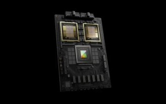
According to news from this website on July 19, TSMC launched the concept of "wafer foundry 2.0" at its second quarter financial report conference held yesterday, further including packaging, testing, photomask manufacturing and other fields, hoping to re- Define the foundry industry. Wei Zhejia said that TSMC's 3 nm and 5 nm demand is strong. This year, AI and smartphones will have great demand for advanced processes. The wafer foundry market will grow by 10% year-on-year in 2024. This site quotes data from research firm TrendForce. According to the traditional definition of foundry, TSMC’s market share in the first quarter was 61.7%.

1. TSMC wafer foundry market share
According to the new wafer foundry definition, TSMC’s wafer foundry business market share in 2023 28%, and is expected to further increase this year.
2. "Wafer Foundry 2.0" Concept
Based on the existing wafer foundry, the "Wafer Foundry 2.0" concept also covers:
- Packaging
- Testing
- Photomask production ( In the IC production process, photolithography technology is used to form patterns on semiconductors)
- IDM industry that does not include memory manufacturing
3. The reason why TSMC promotes "wafer foundry 2.0"
TSMC promotes "wafer foundry 2.0" One of the reasons for "Industry 2.0" is that IDM manufacturers have intervened in the foundry market, and the boundaries of wafer foundry are gradually blurring.

TSMC believes that under the new definition, the wafer manufacturing output value in 2023 will be close to US$250 billion, while the old definition was about US$115 billion.
The above is the detailed content of With an output value of US$250 billion in 2023, TSMC proposes the concept of 'OEM 2.0': covering packaging, testing, photomasks, etc.. For more information, please follow other related articles on the PHP Chinese website!

Hot AI Tools

Undresser.AI Undress
AI-powered app for creating realistic nude photos

AI Clothes Remover
Online AI tool for removing clothes from photos.

Undress AI Tool
Undress images for free

Clothoff.io
AI clothes remover

Video Face Swap
Swap faces in any video effortlessly with our completely free AI face swap tool!

Hot Article
Hot Tools

Notepad++7.3.1
Easy-to-use and free code editor

SublimeText3 Chinese version
Chinese version, very easy to use

Zend Studio 13.0.1
Powerful PHP integrated development environment

Dreamweaver CS6
Visual web development tools

SublimeText3 Mac version
God-level code editing software (SublimeText3)
Hot Topics


 Innolux plans to mass-produce fan-out panel-level semiconductor packaging technology by the end of the year
Aug 07, 2024 pm 06:18 PM
Innolux plans to mass-produce fan-out panel-level semiconductor packaging technology by the end of the year
Aug 07, 2024 pm 06:18 PM
According to news from this site on August 6, Yang Zhuxiang, general manager of Innolux Corporation, said yesterday (August 5) that the company is actively deploying and promoting semiconductor fan-out panel-level packaging (FOPLP) and is expected to mass-produce ChipFirst before the end of this year. The contribution of process technology to revenue will be apparent in the first quarter of next year. Fenye Innolux stated that it is expected to mass-produce the redistribution layer (RDLFirst) process technology for mid-to-high-end products in the next 1-2 years, and will work with partners to develop the most technically difficult glass drilling (TGV) process, which will take another 2-3 years. It can be put into mass production within a year. Yang Zhuxiang said that Innolux’s FOPLP technology is “ready for mass production” and will enter the market with low-end and mid-range products.
 It is reported that TSMC's advanced packaging customers are chasing orders significantly, and monthly production capacity is planned to increase by 120% next year
Nov 13, 2023 pm 12:29 PM
It is reported that TSMC's advanced packaging customers are chasing orders significantly, and monthly production capacity is planned to increase by 120% next year
Nov 13, 2023 pm 12:29 PM
News from this site on November 13, according to Taiwan Economic Daily, TSMC’s CoWoS advanced packaging demand is about to explode. In addition to NVIDIA, which has confirmed expanded orders in October, heavyweight customers such as Apple, AMD, Broadcom, and Marvell have also recently pursued orders significantly. According to reports, TSMC is working hard to accelerate the expansion of CoWoS advanced packaging production capacity to meet the needs of the above-mentioned five major customers. Next year's monthly production capacity is expected to increase by about 20% from the original target to 35,000 pieces. Analysts said that TSMC's five major customers have placed large orders, which shows that artificial intelligence applications have become widely popular, and major manufacturers are interested in artificial intelligence chips. The demand has increased significantly. Inquiries on this site found that the current CoWoS advanced packaging technology is mainly divided into three types - CoWos-S
 TrendForce: Nvidia's Blackwell platform products drive TSMC's CoWoS production capacity to increase by 150% this year
Apr 17, 2024 pm 08:00 PM
TrendForce: Nvidia's Blackwell platform products drive TSMC's CoWoS production capacity to increase by 150% this year
Apr 17, 2024 pm 08:00 PM
According to news from this site on April 17, TrendForce recently released a report, believing that demand for Nvidia's new Blackwell platform products is bullish, and is expected to drive TSMC's total CoWoS packaging production capacity to increase by more than 150% in 2024. NVIDIA Blackwell's new platform products include B-series GPUs and GB200 accelerator cards integrating NVIDIA's own GraceArm CPU. TrendForce confirms that the supply chain is currently very optimistic about GB200. It is estimated that shipments in 2025 are expected to exceed one million units, accounting for 40-50% of Nvidia's high-end GPUs. Nvidia plans to deliver products such as GB200 and B100 in the second half of the year, but upstream wafer packaging must further adopt more complex products.
 It is reported that Zhuang Zishou will be stationed in the United States next month to promote the construction of TSMC's US factory: sprinting to put into production in 2025
Apr 10, 2024 pm 04:52 PM
It is reported that Zhuang Zishou will be stationed in the United States next month to promote the construction of TSMC's US factory: sprinting to put into production in 2025
Apr 10, 2024 pm 04:52 PM
According to news from this website on April 10, according to the Liberty Times, TSMC plans to send Dr. Zhuang Zishou to the United States in May this year to cooperate with Wang Yinglang to jointly promote the construction of TSMC’s US factory. The U.S. Department of Commerce has currently finalized the amount of subsidies for TSMC, Intel, and Samsung, but TSMC's factories in the United States still have many problems. TSMC’s leadership hopes to promote the implementation of advanced processes as soon as possible by sending Dr. Zhuang Zishou to work with Wang Yinglang, who specializes in production and manufacturing. Check out the official TSMC leadership team on this site: Dr. Zhuang Zishou is currently the deputy general manager of factory affairs at TSMC, responsible for the planning, design, construction and maintenance of new factories, as well as the operation and upgrade of existing factory facilities. Dr. Zhuang joined TSMC in 1989 as a
 SK hynix's innovative semiconductor CMP polishing pad technology enables sustainable use
Dec 28, 2023 pm 11:04 PM
SK hynix's innovative semiconductor CMP polishing pad technology enables sustainable use
Dec 28, 2023 pm 11:04 PM
According to news from this website on December 27, according to Korean media ETNews, SK Hynix has recently developed reusable CMP polishing pad technology, which can not only reduce costs, but also enhance ESG (environmental, social, governance) management. SK Hynix said that they will first deploy reusable CMP polishing pads in low-risk processes and gradually expand their application scope. Note: CMP technology is to make the surface of the material to be polished under the combined action of chemicals and mechanics. A process to achieve the required flatness. The chemical components in the polishing fluid react chemically with the material surface to form a softened layer that is easy to polish. The polishing pad and abrasive particles in the polishing fluid physically and mechanically polish the material surface to remove the softened layer. Source: Dinglong shares in CM
 With US$18.12 billion, Nvidia surpassed TSMC and Intel to become the largest revenue producer in the chip industry.
Nov 25, 2023 pm 12:27 PM
With US$18.12 billion, Nvidia surpassed TSMC and Intel to become the largest revenue producer in the chip industry.
Nov 25, 2023 pm 12:27 PM
According to news from this website on November 25, financial analyst Dan Nystedt recently pointed out that based on the financial report data of various companies in the third quarter of 2023, Nvidia surpassed TSMC and Intel and took the top spot in the chip industry revenue. Nvidia’s revenue in the third fiscal quarter was US$18.120 billion (note on this site: currently about 129.377 billion yuan), an increase of 206% compared with US$5.931 billion in the same period last year, and an increase compared with US$13.507 billion in the previous fiscal quarter. 34%. NVIDIA's net profit in the third fiscal quarter was US$9.243 billion (currently approximately 65.995 billion yuan), an increase of 1259% compared with US$680 million in the same period last year, and an increase of 49% compared with US$6.188 billion in the previous fiscal quarter.
 TSMC: The 2nm wafer fab under construction in Nanzi Industrial Park in Kaohsiung, Taiwan has not been affected by Typhoon 'Gemei' and has resumed construction operations
Jul 29, 2024 am 11:58 AM
TSMC: The 2nm wafer fab under construction in Nanzi Industrial Park in Kaohsiung, Taiwan has not been affected by Typhoon 'Gemei' and has resumed construction operations
Jul 29, 2024 am 11:58 AM
According to the news of this website on July 29, according to the Taiwan media "United News Network", due to the impact of Typhoon "Gemei", the 2nm wafer manufacturing factory under construction in Kaohsiung, Taiwan, was temporarily suspended on July 24. The factory has now resumed construction. . ▲Image source Taiwanese media learned after inquiries that Typhoon "Geme" caused widespread flooding in the Kaohsiung area of Taiwan. Nearly 500,000 households lost power, three people died and hundreds of people were injured. However, TSMC stated that the storm did not have a serious impact on its 2nm factory. The Zhuke Baoshan factory in Hsinchu has resumed trial production first. Regarding the Nanzi Industrial Park factory in Kaohsiung, TSMC stated that Typhoon Gemei only caused the collapse of the factory fence. At present, the relevant facilities have been restored. The drainage system and flood detention pond in the factory area were fully functional during the typhoon.
 Sony Group: Its semiconductor factories concealed emissions of harmful substances
Jul 12, 2024 pm 02:09 PM
Sony Group: Its semiconductor factories concealed emissions of harmful substances
Jul 12, 2024 pm 02:09 PM
According to reports from this website on July 8, based on reports from Nikkei and Japan's "Jiji News Agency", on the 8th (today) local time, Sony Semiconductor Manufacturing Company, a semiconductor manufacturer under the Sony Group, announced that the company had discharged harmful chemicals outside the factory. , and no notification was made. The company said this was due to an input error and an imperfect confirmation system. In fiscal years 2021 and 2022, the camera image sensor factory located in Kikuyo Town, Kumamoto Prefecture, incorrectly reported its emissions of chemical substances as 0. The actual situation was that there were emissions of "waste without harmless treatment." The plant emits hydrogen fluoride, which is commonly used in semiconductor processing and cleaning. Note from this site: Hydrogen fluoride is harmful to the human body and can cause respiratory diseases and even life-threatening effects when inhaled. sony half
