
 Technology peripherals
It Industry
Samsung Electronics accused of infringing two Harvard University patents in microprocessor and memory manufacturing
Technology peripherals
It Industry
Samsung Electronics accused of infringing two Harvard University patents in microprocessor and memory manufacturing
Samsung Electronics accused of infringing two Harvard University patents in microprocessor and memory manufacturing

News from this website on August 7, based on reports from Bloomberg Law and Reuters, Harvard University submitted an indictment to the U.S. District Court for the Eastern District of Texas on Monday, accusing Samsung Electronics of infringing two counts of infringement in the fields of microprocessors and memory manufacturing. patent. This website learned from the indictment that Professor Roy G. Gordon of the Department of Chemistry at Harvard University is the inventor of these two patents. Harvard University is the assignee of these patents and has complete rights to the corresponding patents.

▲Samsung office facilities in the United States
These two patents involve deposition methods of cobalt and tungsten-containing films, respectively titled "Cobalt nitride layer for copper interconnects and method of forming the same" and "Nitridation Vapor deposition of tungsten," Harvard University said. "This film is critical to critical components in many products, including computers and cell phones."
Harvard University believes that Samsung Electronics has infringed Harvard University's patents related to the preparation of cobalt nitride films in the process of OEM Qualcomm Snapdragon 8 Gen 1 processors, etc., involving Samsung S22 smartphones and other products.
When Samsung produced LPDDR5X and other memories, it implemented every element of at least one claim in Harvard University's tungsten layer deposition patent without authorization. Samsung's Galaxy Z Flip5 folding screen mobile phone uses the relevant LPDDR5X memory product.

The above is the detailed content of Samsung Electronics accused of infringing two Harvard University patents in microprocessor and memory manufacturing. For more information, please follow other related articles on the PHP Chinese website!

Hot AI Tools

Undresser.AI Undress
AI-powered app for creating realistic nude photos

AI Clothes Remover
Online AI tool for removing clothes from photos.

Undress AI Tool
Undress images for free

Clothoff.io
AI clothes remover

Video Face Swap
Swap faces in any video effortlessly with our completely free AI face swap tool!

Hot Article
Hot Tools

Notepad++7.3.1
Easy-to-use and free code editor

SublimeText3 Chinese version
Chinese version, very easy to use

Zend Studio 13.0.1
Powerful PHP integrated development environment

Dreamweaver CS6
Visual web development tools

SublimeText3 Mac version
God-level code editing software (SublimeText3)
Hot Topics


 Sources say Samsung Electronics and SK Hynix will commercialize stacked mobile memory after 2026
Sep 03, 2024 pm 02:15 PM
Sources say Samsung Electronics and SK Hynix will commercialize stacked mobile memory after 2026
Sep 03, 2024 pm 02:15 PM
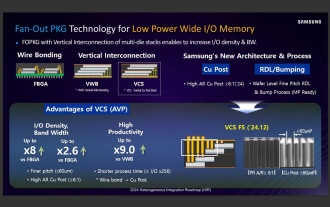
According to news from this website on September 3, Korean media etnews reported yesterday (local time) that Samsung Electronics and SK Hynix’s “HBM-like” stacked structure mobile memory products will be commercialized after 2026. Sources said that the two Korean memory giants regard stacked mobile memory as an important source of future revenue and plan to expand "HBM-like memory" to smartphones, tablets and laptops to provide power for end-side AI. According to previous reports on this site, Samsung Electronics’ product is called LPWide I/O memory, and SK Hynix calls this technology VFO. The two companies have used roughly the same technical route, which is to combine fan-out packaging and vertical channels. Samsung Electronics’ LPWide I/O memory has a bit width of 512
 Samsung announced the completion of 16-layer hybrid bonding stacking process technology verification, which is expected to be widely used in HBM4 memory
Apr 07, 2024 pm 09:19 PM
Samsung announced the completion of 16-layer hybrid bonding stacking process technology verification, which is expected to be widely used in HBM4 memory
Apr 07, 2024 pm 09:19 PM
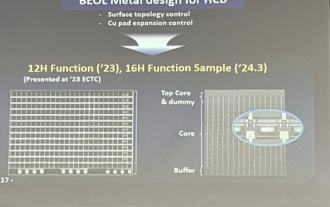
According to the report, Samsung Electronics executive Dae Woo Kim said that at the 2024 Korean Microelectronics and Packaging Society Annual Meeting, Samsung Electronics will complete the verification of the 16-layer hybrid bonding HBM memory technology. It is reported that this technology has passed technical verification. The report also stated that this technical verification will lay the foundation for the development of the memory market in the next few years. DaeWooKim said that Samsung Electronics has successfully manufactured a 16-layer stacked HBM3 memory based on hybrid bonding technology. The memory sample works normally. In the future, the 16-layer stacked hybrid bonding technology will be used for mass production of HBM4 memory. ▲Image source TheElec, same as below. Compared with the existing bonding process, hybrid bonding does not need to add bumps between DRAM memory layers, but directly connects the upper and lower layers copper to copper.
 Transsion responds to Qualcomm's patent infringement lawsuit in India: The agreement has been signed and fulfilled
Jul 18, 2024 pm 03:03 PM
Transsion responds to Qualcomm's patent infringement lawsuit in India: The agreement has been signed and fulfilled
Jul 18, 2024 pm 03:03 PM
According to news on July 13, it was recently reported that Qualcomm is suing Transsion Holdings Group in the Delhi High Court in India, accusing the latter of infringing four of its non-standard essential patents. Transsion responded that it had signed a 5G standard patent license agreement with Qualcomm and was fulfilling the agreement. Transsion said that its sales network covers more than 70 countries in emerging markets such as Africa and South Asia. In some countries, some patent holders do not own or only own a small number of patents. However, it requires a globally unified rate and appeals for excessive licensing fees, which does not take into account the differences in economic development levels in different regions, the fact that it has no patents or only a small number of patents in specific regions or markets, and the existing cases provide different fees in different regions. rate and other factors. This practice does not fully comply with the principles of fairness, reasonableness and non-discrimination. Sound transmission
 Samsung Electronics reiterates that the SF1.4 process is expected to be mass-produced in 2027 and plans to enter the field of co-packaging optics
Jun 13, 2024 pm 05:10 PM
Samsung Electronics reiterates that the SF1.4 process is expected to be mass-produced in 2027 and plans to enter the field of co-packaging optics
Jun 13, 2024 pm 05:10 PM
This site reported on June 13 that Samsung Electronics reiterated at the Samsung Foundry Forum 2024 North America held on June 12, local time, that its SF1.4 process is expected to be mass-produced in 2027, countering previous media rumors. Samsung said its 1.4nm process preparations are progressing smoothly and it is expected to reach mass production milestones in both performance and yield in 2027. In addition, Samsung Electronics is actively researching advanced logic process technology in the post-1.4nm era through innovations in materials and structures to realize Samsung's commitment to continuously surpass Moore's Law. Samsung Electronics simultaneously confirmed that it still plans to mass-produce the second-generation 3nm process SF3 in the second half of 2024. In the more traditional FinFET transistor segment, Samsung Electronics plans to launch S
 It is revealed that Huawei is making its own ultrasonic under-screen fingerprint scanner, and the P80 series is expected to be launched next year
Mar 15, 2024 pm 08:31 PM
It is revealed that Huawei is making its own ultrasonic under-screen fingerprint scanner, and the P80 series is expected to be launched next year
Mar 15, 2024 pm 08:31 PM
With the continuous advancement of mobile phone technology, under-screen fingerprint unlocking has become one of the standard configurations on the market. According to digital blogger @digitalchatstation, Huawei is developing ultrasonic under-screen fingerprint technology, but rumors about Goodix’s patent risks are not entirely true. In addition, Huawei has not only made progress in ultrasonic technology, but also has independently developed algorithm solutions for optical under-screen fingerprints and capacitive fingerprints, showing strong research and development capabilities. It is reported that the current under-screen fingerprint recognition technology mainly includes optical fingerprint recognition and ultrasonic fingerprint recognition. Compared with optical fingerprint recognition, ultrasonic fingerprint recognition technology has the characteristics of fast recognition speed, high recognition rate, strong penetration, no fear of water stains and stains, strong interference ability, support for living body detection, and higher security. It is currently the mainstream flagship machine
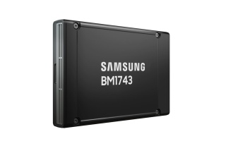 Samsung introduces BM1743 data center-grade SSD: equipped with v7 QLC V-NAND and supports PCIe 5.0
Jun 18, 2024 pm 04:15 PM
Samsung introduces BM1743 data center-grade SSD: equipped with v7 QLC V-NAND and supports PCIe 5.0
Jun 18, 2024 pm 04:15 PM
According to news from this website on June 18, Samsung Semiconductor recently introduced its next-generation data center-grade solid-state drive BM1743 equipped with its latest QLC flash memory (v7) on its technology blog. ▲Samsung QLC data center-grade solid-state drive BM1743 According to TrendForce in April, in the field of QLC data center-grade solid-state drives, only Samsung and Solidigm, a subsidiary of SK Hynix, had passed the enterprise customer verification at that time. Compared with the previous generation v5QLCV-NAND (note on this site: Samsung v6V-NAND does not have QLC products), Samsung v7QLCV-NAND flash memory has almost doubled the number of stacking layers, and the storage density has also been greatly improved. At the same time, the smoothness of v7QLCV-NAND
 Microsoft explores AR/VR patents using microlens arrays for wide-range chief ray angle manipulation
Sep 30, 2023 pm 09:29 PM
Microsoft explores AR/VR patents using microlens arrays for wide-range chief ray angle manipulation
Sep 30, 2023 pm 09:29 PM
(Nweon September 26, 2023) Microsoft believes that MicroLED has the characteristics of small size, light weight, high brightness, and high packaging density, and may be particularly suitable for head-mounted devices that require high resolution, small size, and light weight. monitor. In a patent application titled "Microlenses providing wide range chief ray angle manipulation for panel display", Microsoft introduced a microlens that provides wide range chief ray angle manipulation for panel display, and a display system configured with the microlens array. Wherein, each microlens in the array corresponds to a respective pixel of the panel display. Microlenses are configured according to their
 It is reported that Intel CEO Pat Gelsinger will deliver a plenary speech at ISSCC for the first time next year to introduce foundry progress.
Aug 10, 2024 am 07:42 AM
It is reported that Intel CEO Pat Gelsinger will deliver a plenary speech at ISSCC for the first time next year to introduce foundry progress.
Aug 10, 2024 am 07:42 AM
According to news from this website on August 9, Korean media "Chosun Ilbo" reported that Intel CEO Pat Kissinger will attend the next IEEEISSCC International Solid-State Circuits Conference to be held in San Francisco from February 16th to 20th, 2025 local time. , and will deliver a keynote speech at the ISSCC plenary session for the first time. Note from this site: Speakers at the ISSCC2024 plenary session include Zhang Xiaoqiang, deputy co-chief operating officer of TSMC, etc.; at ISSCC2023, AMD CEO Su Zifeng, imec Chief Strategy Officer JoDeBoeck, etc. delivered plenary speeches. According to reports, Intel’s plenary speakers mainly introduce CPU-related technologies at the ISSCC conference, but Pat Kissinger’s speech to be released next year will focus on Intel’s I
