 Technology peripherals
 It Industry
 Samsung is revealed to start installing its first ASML High-NA EUV lithography machine by the end of 2024 at the earliest
Samsung is revealed to start installing its first ASML High-NA EUV lithography machine by the end of 2024 at the earliest
News from this site on August 16, Seoul Economic Daily reported yesterday (August 15) that Samsung will install the first High-NA EUV lithography machine from ASML between the fourth quarter of 2024 and the first quarter of 2025. , and is expected to be put into use in mid-2025.
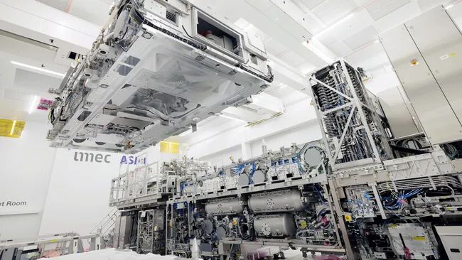
Samsung plans to develop a strong ecosystem around High-NA EUV technology: In addition to acquiring high-NA EUV lithography equipment, Samsung is also collaborating with Japan's Lasertec Corporation to develop inspection equipment specifically for High-NA photomasks.
This site quoted DigiTimes as reporting that Samsung has purchased Lasertec’s High-NA EUV mask inspection tool Actis A300.
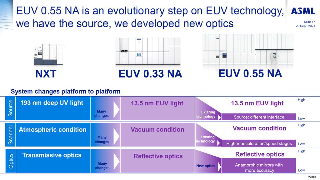
- The report also said that Samsung is also working with photoresist manufacturer JSR and etching machine manufacturer Tokyo Electronics to prepare to put Gaona EUV tools into commercial applications by 2027.
- Samsung is also working with Synopsys to move from traditional circuit designs to curved patterns on photomasks. This shift is expected to improve the precision with which circuits are imprinted on wafers, which is critical to further improving the process technology.
The above is the detailed content of Samsung is revealed to start installing its first ASML High-NA EUV lithography machine by the end of 2024 at the earliest. For more information, please follow other related articles on the PHP Chinese website!

Hot AI Tools

Undresser.AI Undress
AI-powered app for creating realistic nude photos

AI Clothes Remover
Online AI tool for removing clothes from photos.

Undress AI Tool
Undress images for free

Clothoff.io
AI clothes remover

AI Hentai Generator
Generate AI Hentai for free.

Hot Article

Hot Tools

Notepad++7.3.1
Easy-to-use and free code editor

SublimeText3 Chinese version
Chinese version, very easy to use

Zend Studio 13.0.1
Powerful PHP integrated development environment

Dreamweaver CS6
Visual web development tools

SublimeText3 Mac version
God-level code editing software (SublimeText3)

Hot Topics
 1377
1377
 52
52
 Samsung to launch PM1753 data center-grade SSD: 14.8 GB/s sequential read, 3.4 million IOPS random read
Aug 08, 2024 pm 04:40 PM
According to news from this site on August 8, Samsung demonstrated a variety of new SSD products at the 2024 Flash Memory Summit (FMS) - PM1753, BM1743, PM9D3a, PM9E1, and also tested the ninth generation QLCV-NAND, TLCV-NAND and CMM-D –DRAM, CMM-HTM, CMM-HPM, and CMM-BCXL technologies were introduced. BM1743 uses QLC flash memory with a capacity of up to 128TB, a continuous read speed of 7.5GB/s, a write speed of 3.5GB/s, a random read of 1.6 million IOPS, and a write of 45,000 IOPS. It adopts a 2.5-inch form factor and a U.2 interface, and is idle Power consumption is reduced to 4W, and after subsequent OTA updates, only
 Samsung Galaxy S25 Ultra mobile phone leaked: 6.86 inches, horizontal screen-to-body ratio 94.1%
Aug 17, 2024 pm 01:49 PM
According to news on August 17, the source @ibinguniverse posted on Weibo today, stating that the exact size of Apple iPhone 16 Pro Max is 6.88 inches, and the exact size of Galaxy S25 Ultra is 6.86 inches. Both can be regarded as 6.9 inches. Sources indicate that the Samsung Galaxy S25 Ultra has a narrower body and a wider screen than the S24 Ultra, with a horizontal screen-to-body ratio of 94.1%, while the S24 Ultra’s horizontal screen-to-body ratio is 91.5%. Fenye checked the relevant Weibo of the source. He also commented on the newly exposed photos of iPhone 16 Pro Max and believed that it was wrong to be close to a micro-curve. The phone is actually a straight screen + 2.5D glass.
 Samsung's 10,000-yuan foldable phone W25 revealed: 5-megapixel under-screen front camera and thinner body
Aug 23, 2024 pm 12:43 PM
According to news on August 23, Samsung is about to launch a new folding mobile phone W25, which is expected to be unveiled at the end of September. It will make corresponding improvements in the under-screen front camera and body thickness. According to reports, Samsung W25, codenamed Q6A, will be equipped with a 5-megapixel under-screen camera, which is an improvement over the 4-megapixel camera of the Galaxy Z Fold series. In addition, the W25’s external-screen front camera and ultra-wide-angle camera are expected to be 10 million and 12 million pixels respectively. In terms of design, the W25 is about 10 mm thick in the folded state, which is about 2 mm thinner than the standard Galaxy Z Fold 6. In terms of screen, the W25 has an external screen of 6.5 inches and an internal screen of 8 inches, while the Galaxy Z Fold6 has an external screen of 6.3 inches and an internal screen of 8 inches.
 Samsung is revealed to start installing its first ASML High-NA EUV lithography machine by the end of 2024 at the earliest
Aug 16, 2024 am 11:11 AM
According to news from this site on August 16, the Seoul Economic Daily reported yesterday (August 15) that Samsung will install its first High-NAEUV lithography machine from ASML between the fourth quarter of 2024 and the first quarter of 2025. It is expected to be put into use in mid-2025. Reports indicate that Samsung will install the first ASMLTwinscanEXE:5000High-NA lithography machine in its Hwaseong campus, which will be mainly used for research and development purposes to develop next-generation manufacturing technologies for logic and DRAM. Samsung plans to develop a strong ecosystem around High-NAEUV technology: In addition to acquiring high-NAEUV lithography equipment, Samsung is also cooperating with Japan's Lasertec to develop high-NAEUV lithography equipment specifically for High-NAEUV lithography equipment.
 Xiaomi 15 series full codenames revealed: Dada, Haotian, Xuanyuan
Aug 22, 2024 pm 06:47 PM
The Xiaomi Mi 15 series is expected to be officially released in October, and its full series codenames have been exposed in the foreign media MiCode code base. Among them, the flagship Xiaomi Mi 15 Ultra is codenamed "Xuanyuan" (meaning "Xuanyuan"). This name comes from the Yellow Emperor in Chinese mythology, which symbolizes nobility. Xiaomi 15 is codenamed "Dada", while Xiaomi 15Pro is named "Haotian" (meaning "Haotian"). The internal code name of Xiaomi Mi 15S Pro is "dijun", which alludes to Emperor Jun, the creator god of "The Classic of Mountains and Seas". Xiaomi 15Ultra series covers
 A first look at the Samsung Galaxy Z Fold6 / Flip6 mobile phone Gemini Nano AI model: running locally, not yet integrated into Galaxy AI
Aug 10, 2024 pm 01:59 PM
According to news on August 10, technology media Android Authority published a blog post on August 8, stating that Samsung Galaxy Z Fold6 and Galaxy Z Flip 6 have become the first folding phones to support local running of the Gemini Nano AI model. It has not yet been integrated into Galaxy AI. According to reports citing sources, the Galaxy AI and Gemini Nano AI models are two independent systems at this stage. The two have not yet been integrated. Even text-based functions (such as chat assistance, note assistance, text recording assistance or browsing assistance) ) neither. This media test can run GalaxyAI locally without downloading the GeminiNano model: Samsun
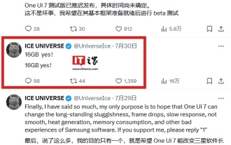 To run Google's Gemini Nano AI model locally, the Samsung Galaxy S25 Ultra phone was revealed to be equipped with 16GB of memory
Jul 31, 2024 pm 05:55 PM
According to news on July 31, the source @ibinguniverse posted a tweet on the Equipped with 16GB of memory. Samsung mobile phone memory capacity update Samsung has launched 16GB memory on Galaxy S20 Ultra and Galaxy S21 Ultra mobile phones. Starting from Galaxy S22 Ultra, including the latest flagship Galaxy S24 Ultra mobile phone, the memory capacity of Samsung mobile phones is capped at 12GB. It is reported that the upcoming Samsung Galaxy S25 and Galaxy S25+ will use 12GB LPDD
 Opening a new chapter in high-quality entertainment: Samsung debuts a variety of e-sports monitors at 2024 ChinaJoy
Jul 29, 2024 pm 04:25 PM
From July 26th to 29th, the 21st China International Digital Interactive Entertainment Exhibition (ChinaJoy) was grandly held at the Shanghai New International Expo Center. As one of the most well-known and influential annual events in the global digital entertainment field, this year's ChinaJoy has the theme of "Travel is where the original intention is, and the excitement is endless", focusing deeply on the integration of technological innovation and digital entertainment. Adhering to the concept of "real players, playing for real", Samsung teamed up with game manufacturers and well-known technology media to create an immersive gaming and entertainment interactive booth for gamers and e-sports enthusiasts, demonstrating Samsung's leading role in promoting technological progress in the gaming industry. , strengthening its role as an important driving force and growth factor for the prosperity and development of the game industry.


