 Common Problem
 What can be done to solve the problem of speed matching between CPU and main memory?
What can be done to solve the problem of speed matching between CPU and main memory?
To solve the problem of speed matching between CPU and main memory, cache memory can be used. Cache memory is a small but high-speed memory located between the CPU and the main memory DRAM. It is usually composed of static memory. Static memory is a small-capacity but high-speed memory located between the CPU and the memory.

The operating environment of this tutorial: Windows 7 system, Dell G3 computer.
In order to solve the problem of speed matching between CPU and main memory, the Cache between the CPU and main memory can be used for its implementation.
What is cache
Cache memory, a cache memory in the computer, is located in the CPU and main memory DRAM (Dynamic Random Access Memory), a smaller but very high-speed memory, usually composed of SRAM (Static Random Access Memory). It is a small-capacity but high-speed memory located between the CPU and the memory.
The speed of the CPU is much higher than that of the memory. When the CPU directly accesses data from the memory, it has to wait for a certain period of time, while the Cache can save a part of the data that the CPU has just used or recycled. If the CPU needs to access data again, When using this part of the data, it can be called directly from the Cache, thus avoiding repeated access to data and reducing the waiting time of the CPU, thus improving the efficiency of the system.
The function of cache
The function of Cache is to increase the rate of CPU data input and output. Cache capacity is small but fast, memory speed is low but capacity is large. By optimizing the scheduling algorithm, the performance of the system will be greatly improved, as if the storage system capacity is equivalent to the memory and the access speed is similar to the Cache.
The speed of the CPU is much higher than that of the memory. When the CPU directly accesses data from the memory, it has to wait for a certain period of time, while the Cache can save a part of the data that the CPU has just used or recycled. If the CPU needs to access data again, When using this part of the data, it can be called directly from the Cache, thus avoiding repeated access to data and reducing the waiting time of the CPU, thus improving the efficiency of the system. Cache is divided into L1Cache (level one cache) and L2Cache (level two cache). L1Cache is mainly integrated inside the CPU, while L2Cache is integrated on the motherboard or CPU.
Basic principles of cache
In addition to SRAM, cache also has control logic. If the cache is outside the CPU chip, its control logic is generally combined with the main memory control logic, called the main memory/chace controller; if the cache is inside the CPU, the CPU provides its control logic.
The data exchange between CPU and cache is in word units, while the data exchange between cache and main memory is in block units. A block consists of several words and is of fixed length. When the CPU reads a word in memory, it sends the memory address of the word to the cache and main memory. At this time, the cache control logic determines whether the word is currently in the cache based on the address: if so, the cache hits and the word is immediately transferred to the CPU; if not, the cache is missing (missed), and the main memory read cycle is used to read the word from the main memory. The read is sent to the CPU. At the same time, the entire data block containing this word is read from the main memory and sent to the cache.
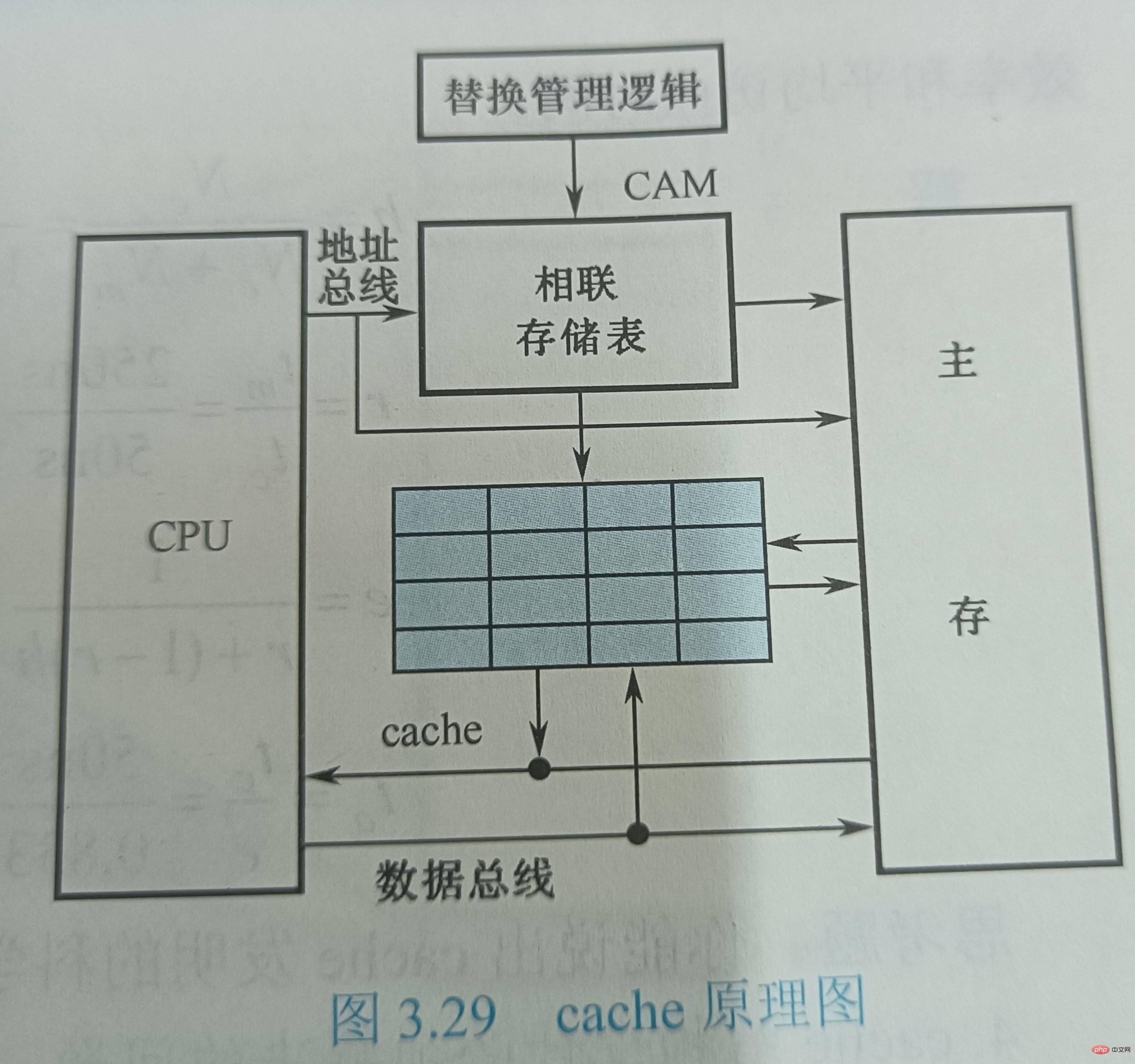
Figure 3.29 shows the schematic diagram of the cache. Assume that the cache read time is 50ns and the main memory read time is 250ns. The storage system is modular, and each 8K module in the main memory is associated with a cache with a capacity of 16 words. The cache is divided into 4 lines, each line has 4 words (W). The address assigned to the cache is stored in an associative memory CAM, which is content-addressable memory. When the CPU executes a memory access instruction, it sends the address of the word to be accessed to the CAM; if W is not in the cache, W is transferred from the main memory to the CPU. At the same time, a row of data consisting of four consecutive words containing W is sent to the cache, replacing the original row of data in the cache. Here, the replacement algorithm is implemented by hardware logic circuits that always manage cache usage.
Problems that must be solved in cache structure design
It can be seen from the basic working principle of cache that the design of cache needs to follow two principles: One is to hope that the cache hit rate is as high as possible, which should actually be close to 1; the other is to hope that the cache is transparent to the CPU, that is, regardless of whether there is a cache, the CPU access memory method is the same, and the software does not need to add anything. The command can access the cache. The hit rate and transparency issues are solved. From the perspective of CPU memory access, the memory will have the capacity of main memory and a speed close to cache. To this end, a certain hardware circuit must be added to complete the control function, that is, the cache controller.
When designing the cache structure, several issues must be solved: ① How to store the contents of the main memory when they are transferred into the cache? ② How to find the information in the cache when accessing the memory? ③ How to replace the cache when the cache space is insufficient What content already exists in the cache? ④ How to rewrite the cache content when a write operation is required?
Among them, the first two questions are related to each other, that is, how to locate the main memory information in the cache, and how to convert the main memory address into a cache address. Compared with the main memory capacity, the cache capacity is very small. The content it saves is only a subset of the main memory content, and the data exchange between the cache and the main memory is in block units. In order to put the main memory block into the cache, some method must be used to locate the main memory address in the cache, which is called address mapping. The physical meaning of the word "mapping" is to determine the corresponding relationship between locations and implement it with hardware. In this way, when the CPU accesses the memory, the memory address of a word given by it will automatically be converted into the cache address, that is, cache address conversion.
The cache replacement problem is mainly to select and execute the replacement algorithm to replace the contents in the cache when the cache misses. The last question involves the cache's write operation strategy, which focuses on maintaining the consistency between the main memory and the cache during updates.
(Learning video sharing: Programming video)
The above is the detailed content of What can be done to solve the problem of speed matching between CPU and main memory?. For more information, please follow other related articles on the PHP Chinese website!

Hot AI Tools

Undresser.AI Undress
AI-powered app for creating realistic nude photos

AI Clothes Remover
Online AI tool for removing clothes from photos.

Undress AI Tool
Undress images for free

Clothoff.io
AI clothes remover

AI Hentai Generator
Generate AI Hentai for free.

Hot Article

Hot Tools

Notepad++7.3.1
Easy-to-use and free code editor

SublimeText3 Chinese version
Chinese version, very easy to use

Zend Studio 13.0.1
Powerful PHP integrated development environment

Dreamweaver CS6
Visual web development tools

SublimeText3 Mac version
God-level code editing software (SublimeText3)

Hot Topics
 1385
1385
 52
52
 What should the CPU utilization be when gaming?
Feb 19, 2024 am 11:21 AM
It's common for games to slow down your computer because they consume a lot of resources. It's crucial to understand your CPU usage when gaming so you can avoid overloading it. Therefore, keeping track of appropriate CPU usage is key to keeping your gaming experience smooth. In this article, we'll look at the appropriate CPU usage you should achieve while your game is running. CPU utilization during gaming CPU utilization is an important indicator of processor workload and depends on the performance specifications of the CPU. More powerful CPUs generally have higher usage. A CPU with more cores and threads can improve the overall performance of your system. Multi-threading support helps unleash the full potential of your CPU. In games, CPU usage depends on processor utilization, which can affect the game
 How to set CPU performance to full in Win11
Feb 19, 2024 pm 07:42 PM
Many users find that the computer is not running smoothly enough when using the Win11 system. They want to improve CPU performance, but they don't know how to do it. The following will introduce in detail how to set the CPU performance to the highest level in Win11 system to make your computer more efficient. Setting method: 1. Right-click "This PC" on the desktop and select "Properties" in the option list. 2. After entering the new interface, click "Advanced System Settings" in "Related Links". 3. In the window that opens, click the "Advanced" tab at the top, then click the & at the bottom of "Performance"
 How to undervolt and overclock your CPU using Intel XTU
Feb 19, 2024 am 11:06 AM
Intel XTU is a powerful application that allows you to easily manage your computer's performance. You can fix overheating issues by adjusting the CPU voltage, or boost performance by overclocking. In this article, we'll look at how you can take advantage of Intel XTU to optimize your computer's performance, whether that's adjusting voltage or overclocking. What effect do undervolting and overclocking have on the CPU? Before we move on to learning how to undervolt and overclock a CPU, we first have to understand what they are. Undervolting refers to gradually reducing the voltage required by the CPU. This process helps reduce heat emissions, as high voltage results in higher temperatures. By reducing the voltage supply to the CPU, the temperature can be effectively reduced. If your laptop starts to slow down after getting hot, you should solve the problem promptly.
 How to increase the clock frequency of your computer's CPU
Feb 20, 2024 am 09:54 AM
How to Overclock Computer CPUs With the continuous advancement of technology, people's demand for computer performance is also getting higher and higher. An effective way to improve computer performance is to increase the CPU's operating frequency through overclocking. Overclocking allows the CPU to process data faster, providing higher computing power. So, how to overclock a computer CPU? The following will introduce you to the basic principles and specific operation methods of overclocking. First, let's understand how overclocking works. The operating frequency of the CPU is determined by the crystal oscillator on the motherboard
 The operation process of WIN10 service host occupying too much CPU
Mar 27, 2024 pm 02:41 PM
1. First, we right-click the blank space of the taskbar and select the [Task Manager] option, or right-click the start logo, and then select the [Task Manager] option. 2. In the opened Task Manager interface, we click the [Services] tab on the far right. 3. In the opened [Service] tab, click the [Open Service] option below. 4. In the [Services] window that opens, right-click the [InternetConnectionSharing(ICS)] service, and then select the [Properties] option. 5. In the properties window that opens, change [Open with] to [Disabled], click [Apply] and then click [OK]. 6. Click the start logo, then click the shutdown button, select [Restart], and complete the computer restart.
 144-core, 3D-stacked SRAM: Fujitsu details next-generation data center processor MONAKA
Jul 29, 2024 am 11:40 AM
According to news from this website on July 28, foreign media TechRader reported that Fujitsu introduced in detail the FUJITSU-MONAKA (hereinafter referred to as MONAKA) processor planned to be shipped in 2027. MONAKACPU is based on the "cloud native 3D many-core" architecture and adopts the Arm instruction set. It is oriented to the data center, edge and telecommunications fields. It is suitable for AI computing and can realize mainframe-level RAS1. Fujitsu said that MONAKA will achieve a leap in energy efficiency and performance: thanks to technologies such as ultra-low voltage (ULV) technology, the CPU can achieve 2 times the energy efficiency of competing products in 2027, and cooling does not require water cooling; in addition, the application performance of the processor It can also reach twice as much as your opponent. In terms of instructions, MONAKA is equipped with vector
 Leak reveals key specs of Intel Arrow Lake-U, -H, -HX and -S
Jun 15, 2024 pm 09:49 PM
IntelArrowLakeisexpectedtobebasedonthesameprocessorarchitectureasLunarLake,meaningthatIntel'sbrandnewLionCoveperformancecoreswillbecombinedwiththeeconomicalSkymontefficiencycores.WhileLunarLakeisonlyavailableasava
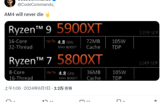 AM4 refuses to die, news says AMD will launch Ryzen 9 5900XT/7 5800XT: clocked at up to 4.8GHz
Jun 05, 2024 pm 09:43 PM
According to news from this website on June 1st, the source @CodeCommando tweeted today, sharing some screenshots of AMD’s upcoming presentation documents at the Computex2024 event. The content of the tweet was “AM4 will never die”, and the accompanying picture showed two new Ryzen5000XT series processors. The screenshots show the following two products: Ryzen 95900 Ryzen75800XT It is a faster variant of AMD's existing Ryzen75800X processor. Both processors are clocked up to 4.8G


