

How is the instruction in the memory sent to the CPU for processing?

If the instructions in the memory are sent to the CPU for processing, it is completed through the "data bus". The bus is a common communication trunk that transmits information between various functional components of the computer; the data bus transmits data that needs to be processed or stored back and forth between the CPU and RAM.

The operating environment of this tutorial: Windows 7 system, Dell G3 computer.
If the instructions in the memory are sent to the CPU for processing, it is completed through the "data bus".
Bus (Bus) is a public communication trunk for transmitting information between various functional components of the computer. It is a transmission harness composed of wires. According to the type of information transmitted by the computer, the bus of the computer can be divided into They are the data bus, address bus and control bus, which are used to transmit data, data address and control signals respectively. The bus is an internal structure. It is a common channel for CPU, memory, input and output devices to transmit information. The various components of the host are connected through the bus, and the external devices are connected to the bus through corresponding interface circuits, thus forming computer hardware. system. In a computer system, the common channel for transmitting information between various components is called a bus. Microcomputers use a bus structure to connect various functional components.
Data Bus: Transfers data that needs to be processed or stored back and forth between the CPU and RAM.
Address Bus: Used to specify the address of data stored in RAM (Random Access Memory).
Control Bus: Transmits signals from the microprocessor control unit (Control Unit) to peripheral devices.
Data Bus (DataBus)
Standardizes the sharing of data between homogeneous and heterogeneous systems in a large integrated application system and exchange implementation methods, data exchange standards between systems. It can be used to transfer information between microprocessor and memory, microprocessor and input and output interface. The width of the data bus is an important indicator of computer performance. Microcomputer data buses are mostly 32-bit or 64-bit.
1. Business entity data exchange: Each subsystem has a business entity layer in the architecture layer. The data exchange mechanism establishes a layer in the business entity layer that is transparent to all application systems. Subsystems, regardless of the specific technical solutions implemented, can share and interact through the business entity layer. This also establishes a structure that can carry out continuous integration and business expansion between subsystems, thereby achieving an scalable a complete integrated information system.
2. WebService data exchange: It is a Web service standard. Web service provides a solution for sharing and exchanging data between heterogeneous systems. It can also be used to use unified interface standards for data sharing and exchange in product integration. exchange.
If you want to read more related articles, please visit PHP Chinese website! !
The above is the detailed content of How is the instruction in the memory sent to the CPU for processing?. For more information, please follow other related articles on the PHP Chinese website!

Hot AI Tools

Undresser.AI Undress
AI-powered app for creating realistic nude photos

AI Clothes Remover
Online AI tool for removing clothes from photos.

Undress AI Tool
Undress images for free

Clothoff.io
AI clothes remover

AI Hentai Generator
Generate AI Hentai for free.

Hot Article
Hot Tools

Notepad++7.3.1
Easy-to-use and free code editor

SublimeText3 Chinese version
Chinese version, very easy to use

Zend Studio 13.0.1
Powerful PHP integrated development environment

Dreamweaver CS6
Visual web development tools

SublimeText3 Mac version
God-level code editing software (SublimeText3)
Hot Topics
 1378
1378
 52
52

 Large memory optimization, what should I do if the computer upgrades to 16g/32g memory speed and there is no change?
Jun 18, 2024 pm 06:51 PM
Large memory optimization, what should I do if the computer upgrades to 16g/32g memory speed and there is no change?
Jun 18, 2024 pm 06:51 PM
For mechanical hard drives or SATA solid-state drives, you will feel the increase in software running speed. If it is an NVME hard drive, you may not feel it. 1. Import the registry into the desktop and create a new text document, copy and paste the following content, save it as 1.reg, then right-click to merge and restart the computer. WindowsRegistryEditorVersion5.00[HKEY_LOCAL_MACHINE\SYSTEM\CurrentControlSet\Control\SessionManager\MemoryManagement]"DisablePagingExecutive"=d
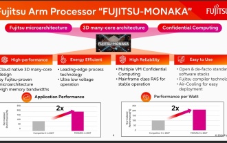 144-core, 3D-stacked SRAM: Fujitsu details next-generation data center processor MONAKA
Jul 29, 2024 am 11:40 AM
144-core, 3D-stacked SRAM: Fujitsu details next-generation data center processor MONAKA
Jul 29, 2024 am 11:40 AM
According to news from this website on July 28, foreign media TechRader reported that Fujitsu introduced in detail the FUJITSU-MONAKA (hereinafter referred to as MONAKA) processor planned to be shipped in 2027. MONAKACPU is based on the "cloud native 3D many-core" architecture and adopts the Arm instruction set. It is oriented to the data center, edge and telecommunications fields. It is suitable for AI computing and can realize mainframe-level RAS1. Fujitsu said that MONAKA will achieve a leap in energy efficiency and performance: thanks to technologies such as ultra-low voltage (ULV) technology, the CPU can achieve 2 times the energy efficiency of competing products in 2027, and cooling does not require water cooling; in addition, the application performance of the processor It can also reach twice as much as your opponent. In terms of instructions, MONAKA is equipped with vector
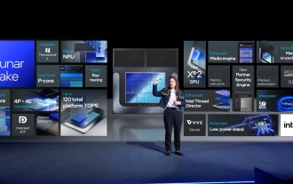 Leak reveals key specs of Intel Arrow Lake-U, -H, -HX and -S
Jun 15, 2024 pm 09:49 PM
Leak reveals key specs of Intel Arrow Lake-U, -H, -HX and -S
Jun 15, 2024 pm 09:49 PM
IntelArrowLakeisexpectedtobebasedonthesameprocessorarchitectureasLunarLake,meaningthatIntel'sbrandnewLionCoveperformancecoreswillbecombinedwiththeeconomicalSkymontefficiencycores.WhileLunarLakeisonlyavailableasava
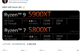 AM4 refuses to die, news says AMD will launch Ryzen 9 5900XT/7 5800XT: clocked at up to 4.8GHz
Jun 05, 2024 pm 09:43 PM
AM4 refuses to die, news says AMD will launch Ryzen 9 5900XT/7 5800XT: clocked at up to 4.8GHz
Jun 05, 2024 pm 09:43 PM
According to news from this website on June 1st, the source @CodeCommando tweeted today, sharing some screenshots of AMD’s upcoming presentation documents at the Computex2024 event. The content of the tweet was “AM4 will never die”, and the accompanying picture showed two new Ryzen5000XT series processors. The screenshots show the following two products: Ryzen 95900 Ryzen75800XT It is a faster variant of AMD's existing Ryzen75800X processor. Both processors are clocked up to 4.8G
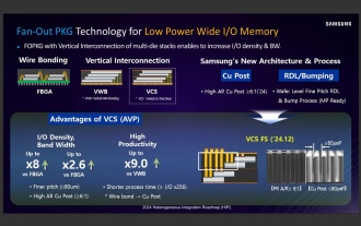 Sources say Samsung Electronics and SK Hynix will commercialize stacked mobile memory after 2026
Sep 03, 2024 pm 02:15 PM
Sources say Samsung Electronics and SK Hynix will commercialize stacked mobile memory after 2026
Sep 03, 2024 pm 02:15 PM
According to news from this website on September 3, Korean media etnews reported yesterday (local time) that Samsung Electronics and SK Hynix’s “HBM-like” stacked structure mobile memory products will be commercialized after 2026. Sources said that the two Korean memory giants regard stacked mobile memory as an important source of future revenue and plan to expand "HBM-like memory" to smartphones, tablets and laptops to provide power for end-side AI. According to previous reports on this site, Samsung Electronics’ product is called LPWide I/O memory, and SK Hynix calls this technology VFO. The two companies have used roughly the same technical route, which is to combine fan-out packaging and vertical channels. Samsung Electronics’ LPWide I/O memory has a bit width of 512
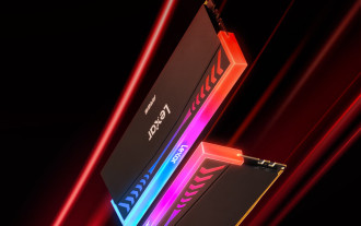 Lexar launches Ares Wings of War DDR5 7600 16GB x2 memory kit: Hynix A-die particles, 1,299 yuan
May 07, 2024 am 08:13 AM
Lexar launches Ares Wings of War DDR5 7600 16GB x2 memory kit: Hynix A-die particles, 1,299 yuan
May 07, 2024 am 08:13 AM
According to news from this website on May 6, Lexar launched the Ares Wings of War series DDR57600CL36 overclocking memory. The 16GBx2 set will be available for pre-sale at 0:00 on May 7 with a deposit of 50 yuan, and the price is 1,299 yuan. Lexar Wings of War memory uses Hynix A-die memory chips, supports Intel XMP3.0, and provides the following two overclocking presets: 7600MT/s: CL36-46-46-961.4V8000MT/s: CL38-48-49 -1001.45V In terms of heat dissipation, this memory set is equipped with a 1.8mm thick all-aluminum heat dissipation vest and is equipped with PMIC's exclusive thermal conductive silicone grease pad. The memory uses 8 high-brightness LED beads and supports 13 RGB lighting modes.
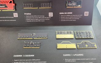 Kingbang launches new DDR5 8600 memory, offering CAMM2, LPCAMM2 and regular models to choose from
Jun 08, 2024 pm 01:35 PM
Kingbang launches new DDR5 8600 memory, offering CAMM2, LPCAMM2 and regular models to choose from
Jun 08, 2024 pm 01:35 PM
According to news from this site on June 7, GEIL launched its latest DDR5 solution at the 2024 Taipei International Computer Show, and provided SO-DIMM, CUDIMM, CSODIMM, CAMM2 and LPCAMM2 versions to choose from. ▲Picture source: Wccftech As shown in the picture, the CAMM2/LPCAMM2 memory exhibited by Jinbang adopts a very compact design, can provide a maximum capacity of 128GB, and a speed of up to 8533MT/s. Some of these products can even be stable on the AMDAM5 platform Overclocked to 9000MT/s without any auxiliary cooling. According to reports, Jinbang’s 2024 Polaris RGBDDR5 series memory can provide up to 8400
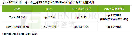 The impact of the AI wave is obvious. TrendForce has revised up its forecast for DRAM memory and NAND flash memory contract price increases this quarter.
May 07, 2024 pm 09:58 PM
The impact of the AI wave is obvious. TrendForce has revised up its forecast for DRAM memory and NAND flash memory contract price increases this quarter.
May 07, 2024 pm 09:58 PM
According to a TrendForce survey report, the AI wave has a significant impact on the DRAM memory and NAND flash memory markets. In this site’s news on May 7, TrendForce said in its latest research report today that the agency has increased the contract price increases for two types of storage products this quarter. Specifically, TrendForce originally estimated that the DRAM memory contract price in the second quarter of 2024 will increase by 3~8%, and now estimates it at 13~18%; in terms of NAND flash memory, the original estimate will increase by 13~18%, and the new estimate is 15%. ~20%, only eMMC/UFS has a lower increase of 10%. ▲Image source TrendForce TrendForce stated that the agency originally expected to continue to