What screen is ltps
LTPS is not a screen, but a process for LCD panels and a production technology. LTPS means "low-temperature polysilicon" in Chinese and is a branch of polysilicon technology. LTPS technology can effectively improve screen operability, and the PPI can reach more than 500. The biggest advantage of ltps screen is that it is ultra-thin, light weight and low power consumption, which can provide more vivid colors and clearer images; it uses laser or heat treatment to melt amorphous silicon, rearrange the crystals and improve mobility, thus Achieve control of high-resolution screens and low power consumption.

The operating environment of this tutorial: Windows 7 system, Dell G3 computer.
LTPS does not refer to the screen, but a process of LCD panels and a production technology.
The full name of ltps is "Low Temperature Poly-silicon", which means "low temperature polysilicon" in Chinese, also referred to as p-Si. It is a branch of polysilicon technology. For LCD displays, the use of polysilicon liquid crystal materials has many advantages, such as thin film circuits that can be made thinner and smaller, lower power consumption, etc.
LTPS technology can effectively improve screen operability, while the PPI can reach more than 500, and is mainly used in mobile phones.
LTPS-TFTLCD LCD displays have the advantages of high resolution, high color saturation, and low cost, and are expected to become a new wave of displays.
The biggest advantage of ltps screen is that it is ultra-thin, light weight and low power consumption, which can provide more vivid colors and clearer images. It uses laser or heat treatment to melt amorphous silicon to rearrange the crystals and increase mobility, thereby achieving control of high-resolution screens and low power consumption.
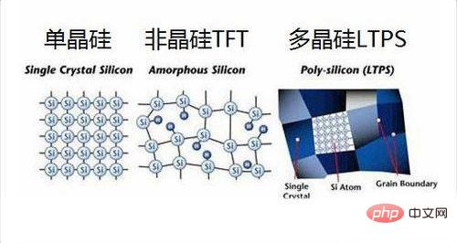
In the early days of the development of polysilicon technology, in order to transform the glass substrate from an amorphous silicon structure (a-Si) to a polysilicon structure, a laser annealing process (Laser Anneal) was necessary. ) high-temperature oxidation process, when the temperature of the glass substrate will exceed 1000 degrees Celsius. As we all know, ordinary glass will soften and melt at this high temperature and cannot be used normally. However, only quartz glass can withstand such high temperature treatment. Quartz glass is not only expensive but also small in size and cannot be used as a display panel. Manufacturers naturally chose cheap amorphous silicon material (a-Si), which is what we see today. However, the industry has not given up its efforts, and the development of low-temperature polysilicon technology has become a consensus. After years of hard work, low-temperature polysilicon has finally gradually become a reality. Compared with traditional high-temperature polysilicon, although low-temperature polysilicon also requires a laser irradiation process, it uses an excimer laser as the heat source. After the laser passes through the transmission system, a laser beam with uniform energy distribution is generated and projected onto the amorphous silicon structure. On the glass substrate, when the glass substrate with amorphous silicon structure absorbs the energy of the excimer laser, it will transform into a polycrystalline silicon structure. Since the entire process is completed below 500-600 degrees Celsius, ordinary glass substrates can also withstand it, which greatly reduces manufacturing costs. It is completely feasible to introduce polysilicon technology into the field of LCD displays. In addition to reduced manufacturing costs, the advantages of low-temperature polysilicon technology are also reflected in the following aspects.
Electron mobility is faster
Electron mobility is measured in "cm2/V-sec", which refers to the movement of electrons per volt per second Range size. Most of the electron mobility indicators of traditional a-Si amorphous silicon material LCD are within 0.5cm2/V-sec, while the electron mobility of P-Si polycrystalline silicon panel can reach 200cm2/V-sec, which is completely higher than that of amorphous silicon material. 400 times as much. Due to the absolute advantage of polysilicon material in this indicator, the response speed of polysilicon LCDs is extremely fast. This is reflected in the shorter response time in display products, which can better meet the practical needs of large-screen LCDs.
Thin film circuit area is smaller
We know that liquid crystal materials display different pictures by controlling the on and off of light. In this way, each liquid crystal pixel must have a Specialized TFT thin film circuit. This thin film circuit corresponds to the liquid crystal pixel one-to-one and becomes part of the pixel. Since the circuit itself is not light-transmitting, the light from the backlight will be blocked by it. The larger the area occupied by the thin film circuit, the less light energy can be transmitted, which is reflected in the darker liquid crystal pixels in the final display. And if the thin film circuit occupies a smaller area, more light will pass through, and the liquid crystal pixels can also have higher output brightness without changing the backlight. The LCD industry introduced the "Aperture Ratio" indicator to describe this situation. The aperture ratio refers to the ratio of the light-transmissible area of each pixel to the total area of the pixel. Obviously, the smaller the area occupied by the thin film circuit, the larger the light-transmissible area, the higher the aperture ratio, and the brighter the overall picture.
The performance of traditional a-Si amorphous silicon materials in terms of aperture ratio is unsatisfactory because the corresponding thin film circuits are relatively large. Although many manufacturers have tried their best to improve this indicator, they have achieved little success. The p-Si polysilicon material has absolute advantages in this regard. For LCD panels made with this technology, thin-film circuits can be made smaller and thinner, and the power consumption of the circuit itself is also lower. More importantly, the smaller thin film circuit allows the polysilicon LCD to have a higher aperture ratio, allowing for better brightness and color output without changing the backlight module. From another perspective, the use of polysilicon materials can effectively reduce the power of the backlight while ensuring that the brightness remains unchanged. The power consumption of the entire machine will therefore be greatly reduced, which is of very positive significance for notebook LCD screens.
Higher resolution
More and more LCD manufacturers are beginning to pay attention to p-Si polysilicon technology. As mentioned before, the size of the thin film circuit of the p-Si polysilicon panel is extremely small, and the aperture ratio is much higher than that of the traditional amorphous silicon panel. It is not only relatively easy to achieve high resolution for the corresponding LCD panel, but also can have better display effect. For example, for a 12-inch notebook LCD screen, if low-temperature polysilicon technology is used, the display can achieve a high resolution of 1024×768 while maintaining the aperture ratio at a level comparable to that of conventional desktop LCD monitors. , thus greatly improving the brightness output, contrast and color effects of the screen, the saying that "there is no good 12-inch screen" will naturally become history. In fact, the resolution that polysilicon technology can achieve is far beyond people’s imagination. For example, in three-chip LCD projectors, high temperature polysilicon (High Temperature Poly-Silicon) technology is widely used, and it can achieve a panel size of only At 1.3 inches, it achieves an ultra-high resolution of 1024×768. If it is replaced by ordinary amorphous silicon technology, it is far from reaching this indicator.
Simple structure and higher stability
For traditional amorphous silicon LCD displays, the driver IC and the glass substrate are separate designs that cannot be integrated. Therefore, in A large number of connectors are required between the driver IC and the glass substrate. Generally speaking, an amorphous silicon LCD panel requires about 4,000 connectors, which inevitably leads to a complicated structure, high module manufacturing costs, poor panel stability, and a relatively high failure rate. . Furthermore, the separate design of the driver IC and the glass substrate also makes it difficult for the LCD to be further thinned, which is a big blow to thin and light laptops and tablet PCs. In contrast, low-temperature polysilicon technology also does not have this problem. The driver IC can be directly integrated with the glass substrate, and the number of required connectors has been reduced to less than 200. The total number of components in the display is 40% less than that of traditional a-Si amorphous silicon technology. This also makes the panel structure simpler and more stable. In theory, the manufacturing cost of polysilicon LCD panels will be lower than traditional technology. At the same time, the integrated structure eliminates the need for the driver IC to occupy additional space, and the LCD display can be made lighter and thinner, which will undoubtedly be widely welcomed by the market.
For more related knowledge, please visit the FAQ column!
The above is the detailed content of What screen is ltps. For more information, please follow other related articles on the PHP Chinese website!

Hot AI Tools

Undresser.AI Undress
AI-powered app for creating realistic nude photos

AI Clothes Remover
Online AI tool for removing clothes from photos.

Undress AI Tool
Undress images for free

Clothoff.io
AI clothes remover

Video Face Swap
Swap faces in any video effortlessly with our completely free AI face swap tool!

Hot Article

Hot Tools

Notepad++7.3.1
Easy-to-use and free code editor

SublimeText3 Chinese version
Chinese version, very easy to use

Zend Studio 13.0.1
Powerful PHP integrated development environment

Dreamweaver CS6
Visual web development tools

SublimeText3 Mac version
God-level code editing software (SublimeText3)

Hot Topics
 1386
1386
 52
52
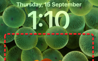 How to show the time under the lock screen wallpaper on iPhone
Dec 18, 2023 am 11:27 AM
Depth Effect is a cool lock screen feature on iOS where part of the wallpaper covers the digital clock. This basically provides a mirage-like effect where the wallpaper appears to be interacting with lock screen elements. In this article, we will explain what the depth effect is all about and how to get the lock screen time/clock behind wallpaper on iPhone. What is the depth effect on iPhone lock screen? Depth effect adds multiple layers of depth to your wallpaper. When you apply a lock screen wallpaper, iOS uses the iPhone's neural network engine to detect depth information in the image you apply. If successful, your iPhone will be able to separate the subject you want to focus on from other elements of the wallpaper. Once a subject is detected, the depth of field effect will
 Teach you how to turn off the automatic screen lock function in win10
Jan 08, 2024 am 11:49 AM
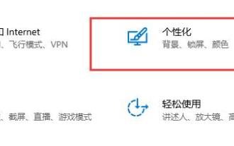
Many friends need to turn off the screen to protect the screen when they leave the computer, but they don’t want to lock the screen because they turn off the screen. When they come back, they have to enter a password to enter the system. In fact, we can complete this step through settings. Let’s take a look at it together. Bar. Tutorial on turning off the screen without locking the screen in win10 1. First enter settings and select "Personalization" 2. Click "Lock Screen" on the left 3. Select "Screen Saver Settings" below 4. Uncheck "Show login on recovery" Screen" 5. Then click "Change Power Settings" 6. Select the icon settings on the left. 7. Set a time to turn off the monitor, and then change the sleep status to "Never" 8. Then return to the power settings just now and select the sleep time below. 9. Use the same as above
 iPhone screenshots not working: How to fix it
May 03, 2024 pm 09:16 PM
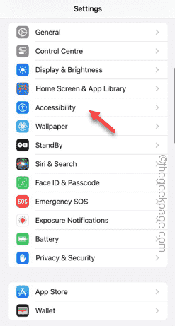
Screenshot feature not working on your iPhone? Taking a screenshot is very easy as you just need to hold down the Volume Up button and the Power button at the same time to grab your phone screen. However, there are other ways to capture frames on the device. Fix 1 – Using Assistive Touch Take a screenshot using the Assistive Touch feature. Step 1 – Go to your phone settings. Step 2 – Next, tap to open Accessibility settings. Step 3 – Open Touch settings. Step 4 – Next, open the Assistive Touch settings. Step 5 – Turn on Assistive Touch on your phone. Step 6 – Open “Customize Top Menu” to access it. Step 7 – Now you just need to link any of these functions to your screen capture. So click on the first
 Does miniled screen hurt eyes?
Feb 07, 2024 pm 03:48 PM
What many users are most concerned about is whether the miniLED screen will hurt the eyes. In fact, although the brightness of this screen can reach extremely high, it will not hurt the eyes and can still be used normally. Does the miniled screen hurt your eyes? Answer: It does not hurt your eyes. Although the brightness of the miniLED screen will be higher, it will not continue to maintain this brightness during daily use. It will only be displayed when the brightness needs to be increased, so it will not always maintain high brightness and hurt the eyes. This peak brightness is also for better Good presentation and expression. MiniLED screen introduction 1. MiniLED backlight display technology uses backlight, so the biggest difference from LCD is the backlight layer 2. Compared with LCD screen, the performance of miniLED will be higher.
 How to adjust the color when the screen turns black and white. Detailed introduction: How to exit black and white mode on your mobile phone.
Mar 21, 2024 pm 01:12 PM
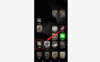
When many friends are using their mobile phones, they suddenly find that the operation interface of the mobile phone has turned into "black and white" color. They don't know what causes it or how to solve it. This article uses Android mobile phones as an example to teach you how to make it work. The color of the mobile phone's operating interface returns to normal. 1. Set up the interface of the mobile phone and find the "gear-shaped" icon in the operation interface. As shown below: Click this icon to enter the phone’s settings interface. 2. Options The operating interface of the mobile phone has changed to black and white, which is related to the "Display" setting of the mobile phone. After entering the settings interface of the mobile phone, find the "Display and Theme" option in the drop-down menu, as shown below: Then click "Display and Theme" option to enter the details page. 3. After changing the screen color and entering the "Display and Theme" option, find the "
 How to Undo Delete from Home Screen in iPhone
Apr 17, 2024 pm 07:37 PM
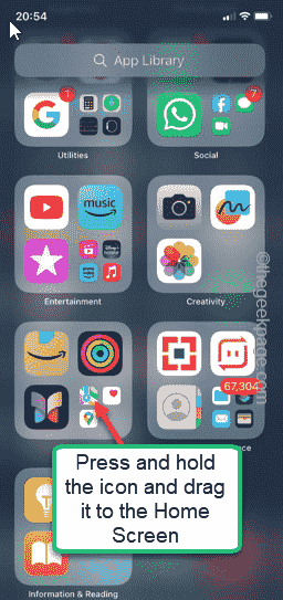
Deleted something important from your home screen and trying to get it back? You can put app icons back on the screen in a variety of ways. We have discussed all the methods you can follow and put the app icon back on the home screen. How to Undo Remove from Home Screen in iPhone As we mentioned before, there are several ways to restore this change on iPhone. Method 1 – Replace App Icon in App Library You can place an app icon on your home screen directly from the App Library. Step 1 – Swipe sideways to find all apps in the app library. Step 2 – Find the app icon you deleted earlier. Step 3 – Simply drag the app icon from the main library to the correct location on the home screen. This is the application diagram
 How to close the 'Do not cover the top of the screen' Detailed explanation: How to close the 'Do not cover the top of the screen' message that appears frequently on your phone
Mar 03, 2024 pm 01:31 PM
I believe many friends have encountered the problem that their mobile phones suddenly prompt: Do not cover the top of the screen. So why does the mobile phone suddenly appear like this? Let’s take a look together below. In fact, when this happens, something is blocking the distance sensor of the phone, so this prompt is received on the screen of the phone. So why did I suddenly receive such a prompt? In fact, it may be that you have accidentally turned on the [anti-accidental touch mode] on your phone, so this problem occurs. So how do we close it? In fact, the method is very simple. Let’s take a look at it together. Method 1: Directly follow the on-screen prompts to close using the shortcut key combination. Method 2: If the above method does not work, you can also open the phone’s [Settings]
 6000 mAh silicon negative battery! Xiaomi 15Pro upgrade leaked again
Jul 24, 2024 pm 12:45 PM
According to news on July 23, blogger Digital Chat Station broke the news that the battery capacity of Xiaomi 15 Pro has been increased to 6000mAh and supports 90W wired flash charging. This will be the Pro model with the largest battery in Xiaomi’s digital series. Digital Chat Station previously revealed that the battery of Xiaomi 15Pro has ultra-high energy density and the silicon content is much higher than that of competing products. After silicon-based batteries are tested on a large scale in 2023, second-generation silicon anode batteries have been identified as the future development direction of the industry. This year will usher in the peak of direct competition. 1. The theoretical gram capacity of silicon can reach 4200mAh/g, which is more than 10 times the gram capacity of graphite (the theoretical gram capacity of graphite is 372mAh/g). For the negative electrode, the capacity when the lithium ion insertion amount reaches the maximum is the theoretical gram capacity, which means that under the same weight


