

How many nanometers is Snapdragon 870?

The Snapdragon 870 is 7nm. Snapdragon 870 is a mobile processing platform chip released by Qualcomm on January 19, 2021. It is made using TSMC’s 7nm process and includes one A77 (3.19GHz) ultra-large core, three A77 (2.42GHz) large cores and four It has an A55 (1.8GHz) performance core, the GPU is Adreno 650, and uses the X55 5G baseband and Spectra 480 ISP.

The operating environment of this tutorial: OriginOS 3 system, iQOO Neo5 mobile phone.
Snapdragon 870 is a mobile phone processor owned by Qualcomm and was officially released on January 19, 2021.
Beijing time on January 19, 2021, Qualcomm officially announced the launch of the Qualcomm Snapdragon 870 5G mobile platform, which is an upgrade of the long-rumored Snapdragon 865 Plus mobile platform. This chip uses the enhanced Qualcomm Kryo 585 CPU core, 7nm process, and the super core frequency has reached 3.2GHz. As of 2021-01-27, it is the highest frequency under the A77 public version architecture.
Officially stated that thanks to Qualcomm Snapdragon Elite Gaming support, 5G Sub-6GHz and millimeter wave support, and intuitive AI features, the new Snapdragon 870 will provide comprehensively improved performance and bring players A better gaming experience.
Kedar Kondap, vice president of product management at Qualcomm Technologies, said: “The new Snapdragon 870 builds on the success of Snapdragon 865 and Snapdragon 865 Plus and will further meet the needs of OEM manufacturers and the mobile industry. . Snapdragon 870 will help leading terminal manufacturers such as Motorola, Xiaomi, OPPO, OnePlus, and iQOO launch a variety of flagship models."

Specification Parameters
The Snapdragon 870 is based on TSMC’s 7nm process and includes one A77 (3.19GHz) ultra-large core, three A77 (2.42GHz) large cores and four A55 (1.8GHz) performance cores. Other aspects include: The Adreno 650 and X55 5G basebands have not changed, but the WIFI chip only supports FastConnect 6800.
The CPU part of the Snapdragon 870 includes 1 A77 (3.19GHz) large core, 3 A77 (2.42GHz) large cores and 4 A55 (1.8GHz) small cores. The GPU is Adreno 650.

Summary
Process: 7nm
CPU architecture: 1 large core 3 The mid-core and 4 small cores have the same architecture as the previous Snapdragon 865 Plus, but the main frequency of the large core has been increased to a terrifying 3.2GHz. The main frequencies of the mid-core and small core have not changed, and are still 2.42GHz and 1.8GHz.
GPU: Adreno 650, the same model as Snapdragon 865 Plus
5G baseband: X55, the same model as Snapdragon 865 Plus
ISP: Spectra 480, the same model as Snapdragon 865 Plus
WiFi: FastConnect 6800 (downgraded), Snapdragon 865 Plus uses the faster one FastConnect 6900
Snapdragon 870 can be called the "Snapdragon 865 Plus" Plus version, because it has only upgraded one large core. However, it should be noted that the positioning of Snapdragon 870 is different from that of Snapdragon 865 Plus. Qualcomm positions it as a sub-flagship SoC.
For more related knowledge, please visit the FAQ column!
The above is the detailed content of How many nanometers is Snapdragon 870?. For more information, please follow other related articles on the PHP Chinese website!

Hot AI Tools

Undresser.AI Undress
AI-powered app for creating realistic nude photos

AI Clothes Remover
Online AI tool for removing clothes from photos.

Undress AI Tool
Undress images for free

Clothoff.io
AI clothes remover

AI Hentai Generator
Generate AI Hentai for free.

Hot Article
Hot Tools

Notepad++7.3.1
Easy-to-use and free code editor

SublimeText3 Chinese version
Chinese version, very easy to use

Zend Studio 13.0.1
Powerful PHP integrated development environment

Dreamweaver CS6
Visual web development tools

SublimeText3 Mac version
God-level code editing software (SublimeText3)
Hot Topics
 1386
1386
 52
52

 AMD Ryzen 9900X, 9700X, 9600X processor Cinebench R23 running scores exposed, with an average increase of 10~15%
Jul 29, 2024 am 11:38 AM
AMD Ryzen 9900X, 9700X, 9600X processor Cinebench R23 running scores exposed, with an average increase of 10~15%
Jul 29, 2024 am 11:38 AM
According to news from this website on July 29, AMD Ryzen 9000 series processors are now available for reservation on JD.com. The first batch of four models will be launched and will be released on August 15. The evaluation data of these processors will be lifted on August 14, the day before they go on sale. However, some media or institutions have obtained samples in advance and started testing, so the running score data of R99900X, R79700X, and R59600X processors have been leaked. ▲Picture source: @9550pro Overall, the move from Zen4 to Zen5 is expected to bring about a 10% to 15% improvement in single-core performance and a 10% to 13% improvement in multi-core performance, but the TDP is somewhat lower than that of the Ryzen 7000 series. Reduced, which is also in line with AMD’s official IPC improvement data. Ryzen
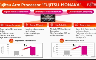 144-core, 3D-stacked SRAM: Fujitsu details next-generation data center processor MONAKA
Jul 29, 2024 am 11:40 AM
144-core, 3D-stacked SRAM: Fujitsu details next-generation data center processor MONAKA
Jul 29, 2024 am 11:40 AM
According to news from this website on July 28, foreign media TechRader reported that Fujitsu introduced in detail the FUJITSU-MONAKA (hereinafter referred to as MONAKA) processor planned to be shipped in 2027. MONAKACPU is based on the "cloud native 3D many-core" architecture and adopts the Arm instruction set. It is oriented to the data center, edge and telecommunications fields. It is suitable for AI computing and can realize mainframe-level RAS1. Fujitsu said that MONAKA will achieve a leap in energy efficiency and performance: thanks to technologies such as ultra-low voltage (ULV) technology, the CPU can achieve 2 times the energy efficiency of competing products in 2027, and cooling does not require water cooling; in addition, the application performance of the processor It can also reach twice as much as your opponent. In terms of instructions, MONAKA is equipped with vector
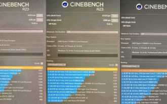
 AMD Ryzen 9 9950X overclocked to 6.6 GHz, CineBench R23 achieved a maximum score of 55296 points
Jul 17, 2024 pm 09:49 PM
AMD Ryzen 9 9950X overclocked to 6.6 GHz, CineBench R23 achieved a maximum score of 55296 points
Jul 17, 2024 pm 09:49 PM
According to news from this website on July 16, the AMDXOC team demonstrated the overclocking Ryzen 99950X processor to the invited media and guests at the Zen5 Technology Day. The processor was overclocked using liquid nitrogen (LN2) and scored more than 5.5 in CineBenchR23. million, and the power consumption is as high as 552W. The overclocking platform used by the XOC team is the ASUS X670EROG CorsshairGene motherboard, which is a motherboard specially designed for overclocking players and equipped with 2 DDR5DIMMs. After using liquid nitrogen, the operating temperature of the Ryzen 99950X processor dropped to minus 90 degrees Celsius, the power consumption was 552W, the CPU was overclocked at 6.4GHz, and the score in CineBenchR23 exceeded 55296
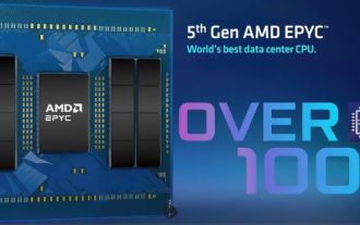 Multi-core exceeds 100,000, AMD EPYC 9755 processor CPU-Z running score exposed: 14% faster than EPYC 9654
Jul 25, 2024 am 10:46 AM
Multi-core exceeds 100,000, AMD EPYC 9755 processor CPU-Z running score exposed: 14% faster than EPYC 9654
Jul 25, 2024 am 10:46 AM
According to news from this website on July 25, the source HXL (@9550pro) tweeted yesterday (July 24), sharing information about the Zen5-based AMDEPYC9755 "Turin" CPU, which achieved excellent results in the CPU-Z benchmark test. score. AMDEPYC9755 "Turin" CPU information EPYC9755 is AMD's fifth-generation EPYC family product, equipped with 128 cores and 256 threads on Zen5 architecture. The base clock frequency of the EPYC9755 processor is 2.70GHz, and the acceleration clock frequency can reach 4.10GHz. Compared with the previous generation, the number of cores/threads has increased by 33%, and the clock frequency has increased by 11%. EPYC9755
 AMD announces 'Sinkclose' high-severity vulnerability, affecting millions of Ryzen and EPYC processors
Aug 10, 2024 pm 10:31 PM
AMD announces 'Sinkclose' high-severity vulnerability, affecting millions of Ryzen and EPYC processors
Aug 10, 2024 pm 10:31 PM
According to news from this site on August 10, AMD officially confirmed that some EPYC and Ryzen processors have a new vulnerability called "Sinkclose" with the code "CVE-2023-31315", which may involve millions of AMD users around the world. So, what is Sinkclose? According to a report by WIRED, the vulnerability allows intruders to run malicious code in "System Management Mode (SMM)." Allegedly, intruders can use a type of malware called a bootkit to take control of the other party's system, and this malware cannot be detected by anti-virus software. Note from this site: System Management Mode (SMM) is a special CPU working mode designed to achieve advanced power management and operating system independent functions.
 AMD Ryzen 7 9700X processor appears on Geekbench: single-core running score is 14% higher than R7 7700X
Jul 12, 2024 pm 01:59 PM
AMD Ryzen 7 9700X processor appears on Geekbench: single-core running score is 14% higher than R7 7700X
Jul 12, 2024 pm 01:59 PM
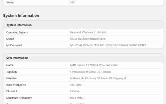
According to news from this website on July 9, an ASUS test machine equipped with AMD Ryzen 79700X processor appeared in the Geekbench database, equipped with ROG CROSSHAIRX670EHERO motherboard and 32GBDDR56000 memory. AMD Ryzen 79700X has 8 cores and 16 threads, 3.8GHz base frequency, 5.5GHz acceleration frequency, 40MB cache (note on this site: 32MBL3+8MBL2) and 65W TDP design, but there is also news that AMD has increased its TDP to 120W. As shown in the figure, the test platform ran single and multi-core scores of 3312 points and 16431 points on Geekbench6.3.0, which is better than R77700.
 2*A78+6*A55, MediaTek releases mid-to-high-end Chromebook processor Kompanio 838
Jun 04, 2024 pm 03:34 PM
2*A78+6*A55, MediaTek releases mid-to-high-end Chromebook processor Kompanio 838
Jun 04, 2024 pm 03:34 PM
According to news from this site on May 31, MediaTek launched the Kompanio 838 processor today. MediaTek said that this 6nm process SoC is aimed at the mid-to-high-end Chromebook market. Compared with the Kompanio500 series products, the graphics performance is improved by up to 76%, the CPU benchmark test is improved by up to 66%, and the Web benchmark test is improved by up to 60%. This site organizes the parameters of the Kompanio838 processor as follows: CPU: 8-core design, 2*ArmCortex-A78@2.6GHz+6*ArmCortex-A55@2.0GHz; GPU: ArmMali-G57MC3; AI processor: NPU650, computing power 4TOPS
 Intel Core Ultra 9 285K processor exposed: single-core running score is 4% faster than Ryzen 9 9950X and multi-core is 14% faster
Aug 21, 2024 pm 04:46 PM
Intel Core Ultra 9 285K processor exposed: single-core running score is 4% faster than Ryzen 9 9950X and multi-core is 14% faster
Aug 21, 2024 pm 04:46 PM
According to news from this website on August 21, technology media WccFtech reported today that the Intel Core Ultra9285K "ArrowLake" processor appeared in the GeekBench6 benchmark library, surpassing the Core i9-14900KS and Ryzen99950X processors. Test platform The test platform exposed this time is ASUS ROGSTRIXZ890-AGamingWIFI motherboard and 64GBDDR5-6400 memory. Introduction to the Intel Core Ultra9285K "ArrowLake-S" desktop processor. The PL1 power consumption of the Intel Core Ultra9285K processor is 125W and it uses a 7nm process (CPU-Z information, it should actually use UK