what is fpga
FPGA is an integrated chip mainly composed of digital circuits, which is a type of programmable logic device (PLD); FPGA is a type and a half in the field of application-specific integrated circuits (ASIC). The emergence of customized circuits not only solves the shortcomings of customized circuits, but also overcomes the shortcomings of the limited number of gates in the original programmable devices.

The operating environment of this tutorial: Windows 7 system, Dell G3 computer.
What is fpga
FPGA (Field Programmable Gate Array) is the basis of programmable devices such as PAL (Programmable Array Logic) and GAL (General Array Logic) product of further development. It appears as a semi-custom circuit in the field of application-specific integrated circuits (ASIC), which not only solves the shortcomings of custom circuits, but also overcomes the shortcomings of the limited number of gates in the original programmable devices.
FPGA is essentially a kind of chip, an integrated chip mainly composed of digital circuits.
FPGA was invented in 1985 by Ross Freeman, one of the founders of Xilinx. It is a type of programmable logic device (PLD). This time is about 20 years later than the emergence of the famous Moore's Law, but once FPGA was invented, the subsequent development speed was faster than most people imagined.
Figure 1 shows the physical picture of the FPGA chip:
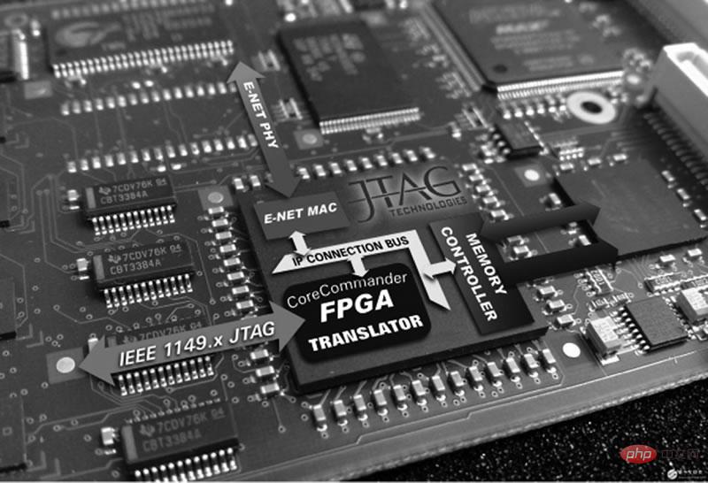
Figure 1 The physical picture of the FPGA chip
FPGA development history
Before the invention of PLD, engineers used discrete logic chips containing several logic gates to build circuit systems. It was difficult to implement complex logic functions.
In order to solve this problem, in the 1970s, the Programmable Logic Array (PLA) came out. The PLA contains a fixed number of AND gates and NOT gates, which form the "AND plane" respectively. ” and “or plane”, that is, “AND connection matrix” and “OR connection matrix”, and the connection matrix that can only be programmed once (because the programming here is based on fuse technology), so some relatively complex AND, or the logical function of multiple expressions, the internal structure of PLA is shown in Figure 2:
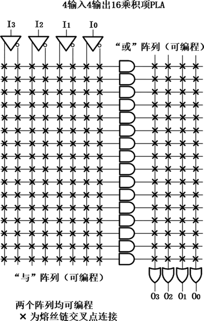
Figure 2 Internal structure of PLA
Also came out at the same time as PLA is programmable Programmable Read-Only Memory (PROM), its internal structure is shown in Figure 3. Like PLA, PROM contains an "AND connection matrix" and an "OR connection matrix" internally, but the connection matrix of the AND gate is fixed in hardware, and only the connection matrix of the OR gate is programmable.
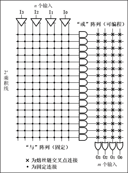
Figure 3 PROM internal structure
If only the connection matrix of the AND gate is programmable, and the connection matrix of the OR gate is fixed by hardware, then this The chip is called Programmable Array Logic (PAL). According to the different working modes of the output circuit, PAL can be divided into three-state output, register output, and complementary output. However, PAL still uses the fuse process and can only be programmed once. . The structure diagram of PAL is shown in Figure 4.
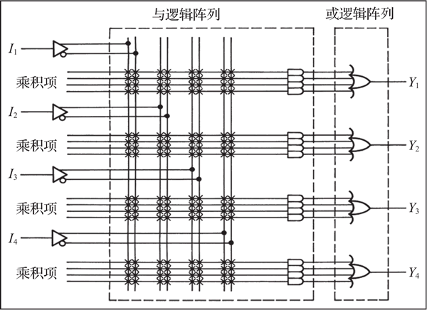
Figure 4 PAL structure diagram
On the basis of PAL, a general array logic device (Generic Array Logic, GAL) has been developed. Compared with Compared with PAL, GAL has two improvements:
- adopts an electrically erasable CMOS process, which can be compiled multiple times, enhancing the reconfigurability and flexibility of the device;
- Adopts a programmable output logic macro cell (Output Logic Macro Cell, OLMC). By programming OLMC, the output of the GAL can be set to different states. Only one model of GAL can realize the working mode of all PAL device output circuits. Enhanced device versatility.
The structure diagram of GAL is shown in Figure 5:
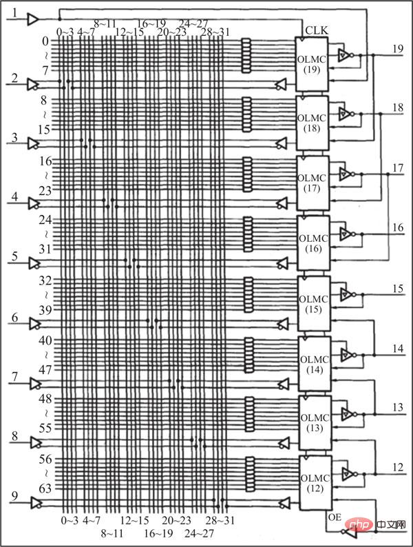
Figure 5 GAL structure diagram
The early PLD was mainly composed of The above four types of chips are composed of PROM, PLA, PAL and GAL. Their common feature is that they can implement logic functions with good speed characteristics, but because their structures are too simple, they can only implement smaller digital circuits.
With the development of science and technology and the progress of society, people have higher and higher requirements for the integration of chips. Early PLD products could not meet people's needs, and Complex Programmable Logic Device (CPLD) was born. CPLD can be viewed as a continuation of the PLA device structure, and a CPLD device can also be viewed as a collection of several PLAs and a programmable connection matrix. The internal structure diagram of CPLD is shown in Figure 6.
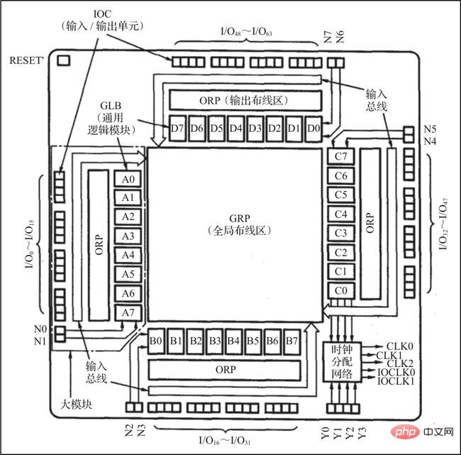
Figure 6 CPLD structure diagram
FPGA came out a few years earlier than CPLD, and is called a high-density programmable logic device together with CPLD, but they are essentially different. The internal architecture of the FPGA chip does not follow a structure similar to PLA, but adopts the concept of Logic Cell Array (LCA), which changes the idea of using a large number of AND gates and NOT gates in PLD devices in the past, mainly using lookup tables. and registers.
In addition, FPGA and CPLD also have differences in resource type, speed, etc., as shown in the table below.
In terms of internal implementation mechanism, the types of FPGA can be divided into based on SRAM technology, based on antifuse technology, and based on EEPROM/Flash technology. In terms of circuit structure, FPGA programmability refers to three aspects of programmability: programmable logic blocks, programmable I/O, and programmable wiring resources. Programmable logic blocks are the core of FPGA programmability, and the three technologies we mentioned above are also technologies for programmable logic blocks.
The structure diagram of FPGA is shown in Figure 7.
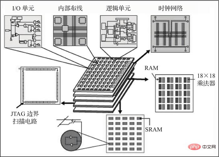
Figure 7 FPGA structure diagram
Technical advantages of FPGA
Many readers know FPGA It’s powerful, but what’s so powerful about it?
Take the microcontroller as an example. We all know that the microcontroller is powerful and can do almost everything, while the FPGA is only stronger than it. Because as long as the functions that the microcontroller can implement, the FPGA can definitely implement them. Of course, this requires a major premise - when the FPGA resources are sufficient. However, the functions that FPGA can realize may not be easily realized by microcontroller. This is an indisputable fact. If you don’t believe it, it only means that you don’t understand FPGA yet.
Speaking of which, readers can’t help but ask, since FPGA is so powerful, why are microcontrollers used more widely? That's because in business, price is often one of the important factors affecting products.
The price of MCU is much lower than that of FPGA, and depending on the performance and resources, the price of FPGA also varies greatly. The price of a single FPGA chip ranges from tens of yuan to hundreds of thousands of yuan. . In comparison, the price of single-chip microcomputer is much cheaper. If we can achieve the same function with a low-priced single-chip computer, we will not choose a relatively expensive FPGA, unless the single-chip computer cannot meet the functional requirements. Therefore, when the company conducts its own development, in order to save costs, it may choose a cheaper microcontroller instead of a relatively expensive FPGA. Because microprocessors such as microcontrollers and ARM are in high demand, the price is more advantageous.
But whether it is a microcontroller, ARM or FPGA, they are just a tool to help us realize functions. The specific choice needs to be analyzed based on specific problems. In short, there are no universal tools, only tools that meet production needs. We should not be biased against a certain tool, but should consider it comprehensively. Likewise, as you learn more, you'll find that these tools all need to be mastered.
The application scenarios of FPGA are far less than that of microcontrollers and ARM, and they mainly target problems that cannot be solved by microcontrollers and ARM. For example, if flexible and efficient, high throughput, low batch latency, fast parallel computing, reconfigurable, reprogrammable, customized performance and customized power consumption are required, these tasks can only be undertaken by FPGA.
Compared with integrated circuits (Application Specific Integrated Circuit, ASIC) designed for special purposes, FPGA has three advantages:
1) Flexibility
By programming an FPGA, the FPGA can perform any logic function that an ASIC can perform. The unique advantage of FPGA lies in its flexibility, that is, the chip function can be changed at any time. This feature can reduce the cost and risk of the product when the technology is not yet mature. This feature is particularly important in the early days of the popularization of 5G technology.
2) Shortened time to market
The FPGA can be used directly after programming. The FPGA solution does not need to go through the chip tape-out cycle of three months to one year, which provides enterprises with Strive for time to market for products.
3) There is a certain cost advantage
The main difference between FPGA and ASIC is that the ASIC solution has fixed costs while the FPGA solution has almost none. When the usage is small, use The FPGA solution does not need to pay millions of dollars in one-time tape-out costs, and it does not need to bear the risk of tape-out failure. At this time, the cost of the FPGA solution is lower than that of ASIC. As the usage increases, the cost advantage of the FPGA solution gradually increases. After a certain amount of usage is reduced, the ASIC solution has more advantages in terms of cost due to the economies of scale produced by a large number of tape-outs, as shown in the following figure:

Figure 8 Cost comparison between FPGA solution and ASIC solution
Therefore, FPGA is usually used in digital signal processing, video processing, image processing, 5G communication field, medical field, industrial control, cloud service, accelerated computing, artificial intelligence, data center , autonomous driving, chip verification and other fields play an irreplaceable role. Only by mastering the general FPGA design method can you make great achievements in the fields where FPGA is unique.
The application direction of FPGA
FPGA is between software and hardware. If you use it for interface and communication, it will favor hardware; use it for For algorithms and control, it tends to be software. With the rise of artificial intelligence and machine vision, FPGAs are more biased towards heterogeneous software algorithms and have the potential to compete with GPUs.
The performance comparison chart between FPGA and GPU is shown in Figure 9:

Figure 9 The performance comparison chart between FPGA and GPU
FPGA software direction: Focus on software development, develop FPGA's accelerated application capabilities in data analysis, artificial intelligence, machine vision and other fields, mainly using OpenCL and HLS technology to achieve collaborative development of software and hardware.
FPGA Hardware Direction: Focusing on logic design, focusing on application design, integrated circuit design and chip verification capabilities in specific fields of FPGA.
The initial application field of FPGA was the communication field. However, with the development of the information industry and microelectronics technology, FPGA technology has become one of the most popular technologies in the information industry, and its application scope has expanded to include aerospace, automobiles, Popular fields such as medical care, broadcasting, testing and measurement, consumer electronics, and industrial control. With the development of technology and advancement of technology, it has begun to penetrate into life from all angles.
For more related knowledge, please visit the FAQ column!
| Device types/characteristics | FPGA | CPLD |
|---|---|---|
| Internal structure | Look Up Table | Product Term |
| Program storage | Internal SRAM structure, external EEPROM or Flash storage program | Internal EEPROM or Flash |
| Resource type | Rich trigger resources | Rich combinational logic resources |
| Integration degree | High | Low |
| Use occasions | Complete more complex algorithms | Complete control logic |
| Generally cannot be kept secret (encryption core can be used) | Can be encrypted |
The above is the detailed content of what is fpga. For more information, please follow other related articles on the PHP Chinese website!

Hot AI Tools

Undresser.AI Undress
AI-powered app for creating realistic nude photos

AI Clothes Remover
Online AI tool for removing clothes from photos.

Undress AI Tool
Undress images for free

Clothoff.io
AI clothes remover

Video Face Swap
Swap faces in any video effortlessly with our completely free AI face swap tool!

Hot Article

Hot Tools

Notepad++7.3.1
Easy-to-use and free code editor

SublimeText3 Chinese version
Chinese version, very easy to use

Zend Studio 13.0.1
Powerful PHP integrated development environment

Dreamweaver CS6
Visual web development tools

SublimeText3 Mac version
God-level code editing software (SublimeText3)

Hot Topics
 Supersega FPGA system aims to hardware emulate half a dozen SEGA systems including SEGA Saturn and SEGA Dreamcast
Jul 01, 2024 am 07:06 AM
The use of Field Programmable Gate Array (FPGA) chips to hardware emulate games has become increasingly popular in recent years. Principally, developers have focused on leveraging FPGA chips for systems released throughout the 1980s and 1990s, includ
 Intel announces the establishment of a new independently operated FPGA company: Altera
Mar 02, 2024 am 09:55 AM
Today, Intel announced the establishment of a new independently operated FPGA company - Altera. During the FPGAVision online seminar held in the morning, CEO Sandra Rivera and COO Shannon Poulin shared their views on how to stay ahead in a market of more than $55 billion, emphasizing that they will achieve this by building FPGAs with integrated AI capabilities. and other initiatives to further enrich the company's product portfolio and also demonstrate that it will continue to help customers cope with increasing challenges. At the meeting, Altera was also officially announced as the brand of the new company. Altera CEO Sandra Rivera said, “At this stage
 what is fpga
Jan 29, 2023 pm 03:59 PM
FPGA is an integrated chip mainly composed of digital circuits, which is a type of programmable logic device (PLD); FPGA appears as a semi-customized circuit in the field of application-specific integrated circuits (ASIC). It not only solves the shortcomings of customized circuits, but also overcomes the shortcomings of the limited number of gate circuits in the original programmable device.
 What are the differences between cpld and fpga
Dec 20, 2023 pm 04:18 PM
The difference between CPLD and FPGA: 1. Structure; 2. Integration level; 3. Interconnection structure; 4. Application scope; 5. Configuration and security; 6. Timing delay. Detailed introduction: 1. Structure, the interior of CPLD is composed of programmable logic units, programmable interconnection and I/O units, and the interior of FPGA is composed of configurable logic blocks, programmable input/output blocks and programmable interconnection matrix; 2 , Integration level, the integration level of CPLD is usually low, and most of them are thousands or tens of thousands of gates in chip scale. In comparison, FPGA has a higher integration level and can reach higher scale, etc.
 AMD launches Spartan UltraScale+ series FPGA products, 16nm FinFET process
Mar 06, 2024 pm 10:40 PM
According to news from this site on March 6, AMD recently launched the Spartan UltraScale+ series of FPGA products for cost-sensitive edge applications. The new generation of Spartan UltraScale+ series FPGAs includes nine products from SU10P to SU200P, which are suitable for I/O expansion, board management, Internet of Things and industrial interconnection scenarios from low to high, and cover the most powerful among AMD's cost-optimized products. Security feature set. AMD claims that Spartan UltraScale+ brings "the industry's highest I/O logic unit ratio" in the field of FPGAs based on 28nm and below process technology, including up to 21,800 logic units and 572 I/Os, with a maximum cost of
 Intel announces that Altera will operate independently, and the $55 billion FPGA market is facing another change
Mar 05, 2024 pm 02:40 PM
On March 1, 2024, Intel announced the establishment of a new independently operated FPGA company-Altera. Altera, which operates independently, plans to conduct a public offering (IPO) within the next 2-3 years. Previously, Sandra Rivera, general manager of Intel's Data Center and Artificial Intelligence (DCAI) Division, served as CEO of the independently operated Altera company. Intel acquired Altera for US$16.7 billion in June 2015. Altera was the world's second largest FPGA company when it was acquired. Nine years later, Intel decided to let the FPGA business operate independently and once again used Altera as the company name. It felt like rebirth of Altera. . For Altera's independent operation, Arr
 Intel spins off independent FPGA company Altera: sorting out and upgrading Agilex product line, chasing US$55 billion opportunity
Mar 01, 2024 pm 05:00 PM
According to news from this site on March 1, Intel Corporation issued a press release today, announcing the official establishment of FPGA90 (field programmable gate array) company Altera in an independent development model, and launched Agilex9, Agilex7F series and I series, Agilex5 and Agilex3, etc. product. Altera CEO Sandra Rivera and COO Shannon Poulin unveiled their strategy to pursue a market opportunity of more than $55 billion. Rivera said during the live event that the company sees an opportunity to reinvigorate the FPGA market. She said Altera will strive to lead the market with a "bold, agile and customer-centric approach" to develop products for different applications.
 New refresh of popular retro gaming handheld announced with strong Game Boy Color vibes
Sep 12, 2024 pm 12:17 PM
Analogue has once again refreshed the Pocket, roughly two months after it updated the device with aluminium options. Unfortunately, it seems that the company remains content with releasing limited-run versions of a device that it announced almost fiv


