To say Tesla is only interested in machine learning would be an understatement. In fact, the electric car maker built an in-house supercomputer called Dojo, optimized for training its machine learning models.
Unlike many other supercomputers, Dojo does not use off-the-shelf CPUs and GPUs, such as those from AMD, Intel, or Nvidia. Tesla designed its microarchitecture based on their needs, allowing them to make tradeoffs that more general-purpose architectures couldn't.
In this article, we’ll take a look at the architecture based on Tesla’s demonstration at Hot Chips. The architecture does not have a separate name, so for simplicity, whenever we refer to Dojo in the following, we are talking about the architecture.
#At a high level, Dojo is an 8-wide core with four-way SMT running at a conservative 2 GHz, Having a CPU-style pipeline makes it more tolerant of different algorithms and branching codes than a GPU. Dojo's instruction set is similar to RISC-V in scalar terms, but Tesla engineers added a custom set of vector instructions focused on accelerating machine learning.
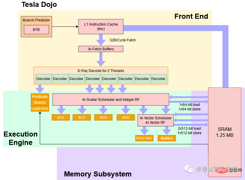
#Simplified block diagram of Tesla Dojo core
Tesla describes Dojo as a "high-throughput, general-purpose CPU." From a performance perspective, there's definitely some truth to this. But in order to increase computing density, Tesla made a sacrifice, and Dojo cores are very difficult to use compared to the CPUs we are familiar with in desktops, laptops, and smartphones. In some ways, the Dojo kernel handles things more like the SPE in IBM's Cell than a traditional general-purpose CPU kernel.
Introduced in the mid-2000s, the IBM Cell processor features eight "Synergistic Processing Elements" or SPEs, consisting of a fully functional CPU core ("Power Processing Element"). ” or PPE: Power Processing Element) control. At first glance, Dojo has many similarities with SPE.
Both Dojo and SPE are optimized for vector processing and rely on a separate host processor for work distribution. Code running on Dojo or SPE cannot directly access system memory. Instead, applications are expected to work primarily in a small portion of local SRAM. This local SRAM is managed by software and cannot be used as cache. If data from main memory is required, it must be brought in using a DMA operation.
Finally, both Dojo and Cell's SPE lack support for virtual memory. We'll get into the details of what this means later, but in short, it makes multitasking very difficult.
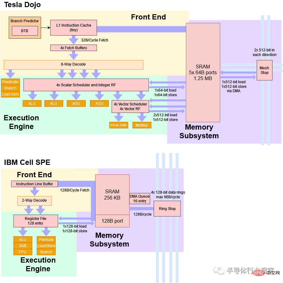
##A very simplified comparison between Tesla Dojo and IBM Cell SPE
Dojo is different in several important ways. Because Dojo was not designed with small-scale deployments in mind, the host processor resides on a separate host system. These host systems have PCIe cards with interface processors, which are then connected to the Dojo chips via high-speed network links. In contrast, Cell's main processor resides on the same chip. This makes it possible to deploy individual Cell chips individually - something that is not possible in Dojo.Dojo's 1.25 MB local block of SRAM is much larger and has higher bandwidth than the Cell SPE which only has 256 KB of SRAM. Cell's 256 KB SRAM has only one port, capable of delivering 128B per cycle. Dojo's SRAM has five 64B ports. Of course, the architectural goals are very different. Dojo is wide clocked and low clocked, while Cell SPE has narrow and deep pipelines designed for high clocked.
Let us briefly introduce Dojo pipelines starting from the front end. There is some kind of branch predictor, as Tesla's diagram shows BTB (branch target buffer: branch target buffer). Its predictive capabilities may not reach the level we see on high-performance cores from AMD, ARM, and Intel, because Dojo needs to prioritize spending die area on vector execution. But even a basic branch predictor is a big improvement over no predictor, and Dojo's branch prediction capabilities should provide better performance than the GPU when dealing with branched code or larger instruction footprints. Once the branch predictor generates the next instruction fetch pointer, Dojo can fetch 32 bytes per cycle from the "small" instruction cache into each thread's fetch buffer (per-thread fetch buffers). This instruction cache may help reduce instruction bandwidth pressure on the local SRAM, ensuring that the data side can access the SRAM with as little contention as possible. Additionally, the instruction cache is not coherent. If new code is loaded into local SRAM, the instruction cache must be flushed before branching to the new code. #Hot Chips Presentation from Tesla From the fetch buffer, Dojo's decoder can process eight instructions per cycle from two threads. I'm a little confused about what "two threads per cycle" means, since CPUs with SMT typically handle one thread per cycle and switch threads on cycle boundaries. Maybe Dojo splits the decoder into two clusters and selects two threads to feed them data in each loop. This may reduce the decoding throughput penalty for the branch taken. While decoding, certain instructions (such as branches, predicated operations and immediate loads ("list parsing")) can be executed on the front end and removed from the pipeline. This is a bit like newer x86 CPUs that eliminate register-to-register copies in the renamer. But you heard that right - Dojo does not track "eliminate" instructions through the pipeline to maintain in-order retirement. Other processors track everything to exit so that they can stop at any instruction boundary and maintain all the state needed to resume execution. This ability is called "precise exceptions", and modern operating systems use it to provide all kinds of goodies, like paging to disk, or telling you exactly where your code is messed up. Tesla doesn’t care about precise exceptions. Dojo does have a debug mode where more instructions are passed through the pipeline to provide "more precise" exceptions, but there is no orderly exit logic like a normal out-of-order CPU. After seeing a wide front-end, see a 4-wide with only two ALUs and two AGUs The integer execution engine can be a bit strange. But this funnel-shaped pipeline makes sense because some instructions are executed and discarded on the front end. Dojo also won't make it into client systems where scalar integer performance is important. Therefore, the integer side provides sufficient throughput to handle control flow and address generation to keep vector and matrix cells fed. Dojo’s vector and matrix execution ends are placed after the scalar execution engine in the core pipeline, and there are two execution pipelines. Two pipelines may not sound like much, but Dojo has very wide execution units behind these pipelines. One pipeline can perform 512-bit vector execution, while the other pipeline performs 8x8x4 matrix multiplication. Therefore, as long as the instructions expose enough explicit parallelism, Dojo can achieve very high throughput - especially if matrix units are used. Tesla claims that a chip with 354 Dojo cores can achieve 362 BF16 TFLOPS at 2 GHz, which suggests that each core can perform 512 BF16 FLOPS per cycle. We are not sure if Dojo can be executed completely out of order. But Tesla did say that the integer side can run far ahead of the vector side, suggesting it could execute instructions that used to stall until one of the schedulers filled up. The lack of ordered retirement also points to out-of-order execution capabilities. Generally, implementing out-of-order execution brings a lot of complexity. This is because the CPU must execute instructions in sequence. High-performance CPUs from AMD, ARM, and Intel use large reorder buffers (and other structures) to keep track of instructions so that their results can be committed in program order. This means that if a program does something stupid, like divide by zero, these cores can show exactly which instruction went wrong. Furthermore, they can display a CPU state that reflects the actions of all instructions before the fault, but not after. This means you can fix whatever caused the instruction to go wrong and resume execution. Dojo gives up this ability. In exchange, Dojo avoids the power and area overhead associated with tracking each instruction through its pipeline to ensure results are delivered in program order. Normally, we would talk about caching here. But Dojo does not have direct access to system memory, so we will discuss the 1.25 MB block of SRAM. It can handle two 512-bit loads per cycle, giving it bandwidth per cycle that matches AVX-512-capable Intel CPUs. Tesla says the SRAM has five 512-bit ports (2 load ports, 1 store port, and two stop-to-grid ports). But there are only two AGUs on the scalar side, which probably means the core can't handle two 512-bit loads and one 512-bit store per cycle. Because Dojo's local SRAM block is not cached, it does not require the tag and status bits stored with the data. SRAM also doesn't have an L1D cache in front of it, so it has to be fast enough to handle all load and store instructions without causing a bottleneck, even though it's closer in size to the L2 cache. Not implementing SRAM as a cache may be Tesla's way of keeping latency low. If we look back to AMD's Hammer architecture from long ago, we can see that it took 8 cycles to access 1 MB of L2 after detecting an L1D miss (for a total latency of 12 cycles). If 1 MB of SRAM were addressed directly rather than used as cache, three stages might be removed, lowering latency to 5 cycles: From an older Hot Chips demo This slide shows the pipeline stages involved in L2 cache access. If L2 is not a cache, stages that can be skipped are marked in red. Given decades of process node improvements and even lower clock speed targets than Athlon, it's easy to see how Tesla could access L2-sized SRAM with L1-like latency piece. Skipping the L1 cache certainly saves area and power. To further reduce latency, area, and core complexity, Dojo has no virtual memory support. Therefore, it has no TLB or page walk mechanisms. Modern operating systems utilize virtual memory to give each process its own view of memory. The memory address used by the program is not a direct access to the physical memory address, but is converted to a physical address by the CPU using the paging structure set by the operating system. This is how modern operating systems isolate programs from each other and prevent one misbehaving application from bringing down the entire system. Virtual memory is also how you can run more programs than you have in physical memory. When you run out of real memory, the operating system unmaps the page, writes it to disk, and gives your program the memory it needs. When some other crappy program tries to access that memory, the CPU tries to translate the virtual address to a physical address, but finds that the translation doesn't exist. The CPU throws a page fault exception, which the operating system handles by reading the evicted page back into physical memory and filling in the page table entry. None of this is possible on Dojo. The kernel's 4-way SMT feature is more about exposing a single application to explicit parallelism than improving multitasking performance. For example, one thread can perform vector calculations while another thread asynchronously loads data from system memory to SRAM (via DMA). To further simplify the design, Dojo can address SRAM with only 21 address bits, which can simplify Dojo's AGU and addressing bus. These trade-offs could allow Tesla to access this SRAM with low enough latency to avoid implementing a separate L1 data cache in front of it. Speaking of system memory, the Dojo chip is not directly connected to the memory. Instead, they connect to an interface processor equipped with an HBM. These interface processors are also responsible for communicating with the host system. Dojo tile with 25 independent chips can access 160 GB of HBM memory Tesla says they can access 160 GB of HBM memory across tile boundaries from each The chip edge transfers 900 GB/s, which means the interface processor and its HBM can be accessed with 4.5 TB/s link bandwidth. Because access to the HBM requires going through a separate chip, access latency can be very high. Dojo is an 8-wide kernel with at least some OoO execution capabilities, decent vector throughput, and a matrix multiplication unit. But even with 1.25 MB of local SRAM, it ends up being a very small core. In comparison, Fujitsu's A64FX occupies more than twice the area on the same process node. Processor design is all about making the right trade-offs. Tesla wants to maximize machine learning throughput by packing a large number of cores onto a chip, so individual cores must be small. To achieve its zone efficiency, Dojo uses some familiar techniques. It runs at a conservative 2 GHz. Lower clock circuits tend to occupy less area. It might have a basic branch predictor and a small instruction cache. If the program has a large code footprint or has many branches, this will sacrifice some performance. But Tesla also further reduces power and area usage by cutting out features not needed to run internal workloads. They do not do data-side caching, do not support virtual memory, and do not support precise exceptions. #The result is a processor core that offers the performance flexibility of modern CPU cores while being inferior in many aspects to the Intel 8086 User and programmer friendly. In addition to the core, Tesla is also saving chip area at scale by designing Dojo chips specifically for deployment. Shrinking, the Dojo core is implemented on a very large 645 mm2 die called D1. Unlike other chips we are familiar with, a single Dojo chip is not self-sufficient. It doesn't have a DDR or PCIe controller. There are IO interfaces around the edges of the die that allow the die to communicate with adjacent dies with a latency of about 100 ns. To access system memory, the Dojo D1 chip must communicate with an interface processor that has an onboard HBM. The interface processor is in turn connected to the host system via PCIe (the interface processor is installed on a PCIe card). In theory, a minimal functional Dojo deployment would involve a Dojo chip, an interface processor card, and a host system. But Tesla deploys Dojo dies in modules containing 25 dies each to provide a sense of scale. The Dojo D1 die is specifically designed to be a building block for supercomputers and nothing more. This specialization can save more die area. Dojo D1 does not waste space on DDR and PCIe controller. Most of the die is taken up by the massive Dojo core, except for the custom IO connectors on the outside designed to interface with the adjacent die. # In contrast, chips designed with more deployment flexibility in mind spend a lot of space on IO . AMD’s Zen 1 “Zeppelin” chips demonstrate this very well. Zeppelin can connect directly to DDR4 memory, PCIe devices, SATA drives and USB devices – perfect for customer requirements. In a server, the IFOP interface allows it to communicate with adjacent chips. Large chunks of SRAM located near the IFOP may be snoop filters, helping to maintain cache coherence efficiently in high core count settings. Dojo does not attempt to maintain cache coherence across cores, and does not use any SRAM for snoop filtering. ##From AMD’s chiplet demo at ISSCC 2021 AMD pays for this flexibility by devoting approximately 44% of the "Zeppelin" die area to logic other than cores and cache. Dojo uses only 28.9% of the die area for things other than SRAM and cores. The microarchitecture behind the Tesla Dojo supercomputer shows how to achieve very high computational density while still maintaining a CPU Ability to handle branched code. To get there, you need to give up most of the comforts that define our modern computing experience. If you can hypothetically build your desktop around the Dojo core, the experience will probably feel familiar to anyone who has used MS-DOS. You cannot run multiple applications at the same time. A single misbehaving application may force you to reboot your system. If you don't have enough RAM to run a program, you can forget about running it entirely (without paging to disk). But these trade-offs make perfect sense in Tesla’s supercomputer. Tesla does not require a Dojo core to handle multiple running applications simultaneously, Dojo only needs to run trusted code within. So, Tesla doesn't care about virtual memory support. Likewise, machine learning programs running on Dojo will be written with that specific system in mind. You won't have a batch of arbitrary programs that might require more memory than is available. This means you don't need precise exceptions (and virtual memory) to allow techniques such as overcommitting memory, memory compression, or swapping memory pages between disks. Precise exceptions are also useful for debugging, but Tesla does it in a cheaper way through a separate debug mode. # To be sure, the trade-offs Tesla has made to achieve high compute density are not possible in consumer or server CPUs . But they're a lot of fun in action, and we have to thank Tesla for taking the time to show them off at Hot Chips. Over the past two decades, improvements in process nodes have been slowing, resulting in even slower progress in single-threaded performance. Power and cooling constraints have been reducing multi-threaded performance for the past five years. But the need for more computing power isn't slowing down, so companies are turning to more specialized hardware to keep pace. The architecture in Tesla’s Dojo supercomputer is a good example of how trade-offs are made to increase computational density and how current trends favor serving throughput-constrained applications The program introduces specialized hardware. Front end: CPU Comforts, etc.

Dojo's execution engine
SRAM Access
Memory Access

is small, how to do it?

Physical Implementation


Final Words
The above is the detailed content of Inspiration from Tesla's self-developed chip architecture. For more information, please follow other related articles on the PHP Chinese website!


