
 Technology peripherals
AI
The 1 trillion semiconductor industry support plan is here! my country's chip self-sufficiency takes the first step
Technology peripherals
AI
The 1 trillion semiconductor industry support plan is here! my country's chip self-sufficiency takes the first step
The 1 trillion semiconductor industry support plan is here! my country's chip self-sufficiency takes the first step

Recently, the United States has tightened its grip on my country, and has also roped in the Netherlands and Japan with the intention of forming a "Triple Alliance."
In response, our country is formulating a semiconductor industry support plan of more than 1 trillion yuan ($143 billion).
This is an important step towards my country’s self-sufficiency in chips.
The plan is being formulated
It is said that this 1 trillion industrial support plan is one of the largest financial incentive plans in recent times, with an allocation period of five years. Domestic semiconductor production and research activities are supported through subsidies and tax credits.
As demand for chips soars, our country will take a more direct approach to shaping the future of this industry.
This may further cause the United States and its allies to worry about my country’s competition in the semiconductor industry.
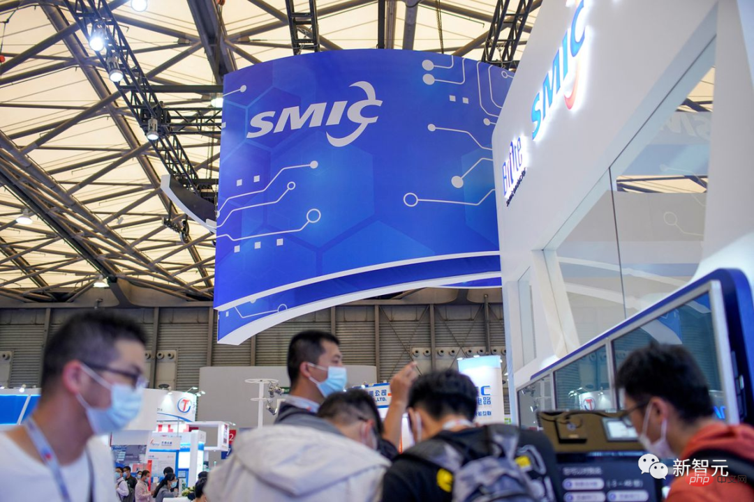
People are visiting the China International Semiconductor Expo (IC China 2020) in Shanghai on October 14, 2020 Core International’s booth
# Some U.S. lawmakers have begun to worry about my country’s chip production capacity construction.
It is reported that this plan may be implemented as early as the first quarter of next year.
According to the plan, most of the financial aid will be used to subsidize Chinese companies to purchase domestic semiconductor equipment, mainly semiconductor manufacturing plants or wafer fabs. These companies will be entitled to a 20% subsidy on procurement costs.
This incentive program aims to increase the construction and expansion of my country's chip companies, as well as support for manufacturing, assembly, packaging and R&D facilities.
In addition, China’s semiconductor industry will also enjoy preferential tax policies.
Chip Bill
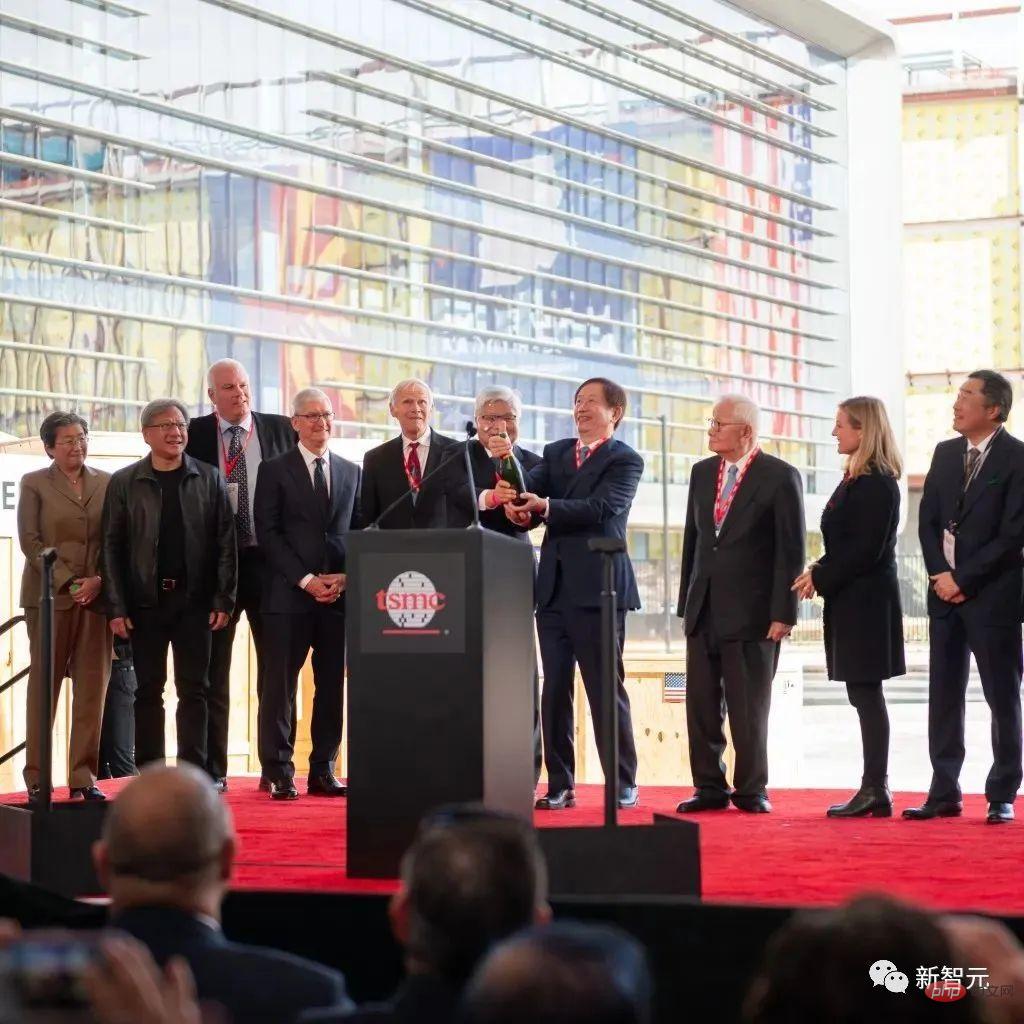
On December 7, AMD Chairman Lisa Su, NVIDIA founder Jen-Hsun Huang, Apple CEO Cook, TSMC founder Zhang Zhongmou, etc. were on the same stage. Celebrating the launch of TSMC’s first U.S. factory.
In October this year, the U.S. Department of Commerce passed a sweeping set of regulations that prohibit certain research laboratories and commercial data centers from obtaining advanced artificial intelligence Smart chips also include other restrictions.
At the same time, the United States has also been lobbying partners, including Japan and the Netherlands, to tighten exports of equipment used to make semiconductors to China.
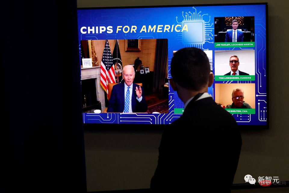
In August this year, Biden signed the landmark chip bill, which provided US$52.7 billion in funding for semiconductor production and research in the United States, and provided chips valued at US$24 billion. Factory tax credits are available.
#Who will benefit?
Beneficiaries of this plan include state-owned and private enterprises in the chip industry, especially large semiconductor equipment companies, such as Northern Huachuang Technology Group, Advanced Micro Manufacturing Equipment Co., Ltd. and Gold Semiconductor .
Shares of Chinese chipmakers surged in early trading on Wednesday after the news broke.
China's Shanghai Science and Technology Innovation Board index opened up nearly 4%. The share price of industry giant Semiconductor Manufacturing International Corporation (SMIC) rose 5.2% to a four-month high.
Some Chinese chip Hong Kong stocks also rose sharply on Tuesday. SMIC rose more than 8% and gained nearly 10% throughout the day. Hua Hong Semiconductor closed up 17%.
On February 29, 2016, at the Research Center of Tsinghua Unigroup, a researcher implanted a semiconductor into a Interface board
#The sanctions announced by the United States in October have caused major overseas chip manufacturing equipment companies to stop supplying to Chinese chip manufacturers, including Yangtze Memory and China Core International.
In addition, some advanced artificial intelligence chip manufacturers have also stopped supplying to Chinese companies and laboratories.
Now, our country is still lagging behind in the field of chip manufacturing equipment, which is still dominated by companies from the United States, Japan and the Netherlands.
Over the past 20 years, many domestic companies have emerged in our country, but most still lag behind their competitors in their ability to produce advanced chips.
For example, Northern Huachuang’s etching and thermal process equipment has relatively mature technology, but it can only produce chips of 28 nanometers and above.
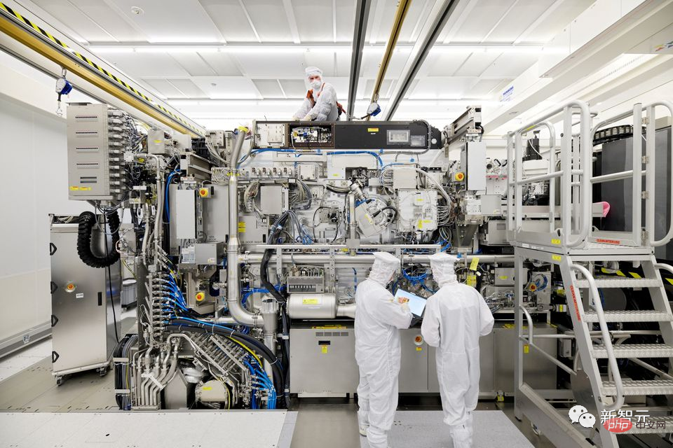
On April 4, 2019, employees performed the final assembly of ASML’s TWINSCAN NXE:3400B semiconductor lithography tool in Veldhoven, the Netherlands
Shanghai Microelectronics Equipment Group Co., Ltd. is the only photolithography company in my country that can produce 90-nanometer chips, but ASML in the Netherlands can already produce chips as low as 3 nanometers. .
The above is the detailed content of The 1 trillion semiconductor industry support plan is here! my country's chip self-sufficiency takes the first step. For more information, please follow other related articles on the PHP Chinese website!

Hot AI Tools

Undresser.AI Undress
AI-powered app for creating realistic nude photos

AI Clothes Remover
Online AI tool for removing clothes from photos.

Undress AI Tool
Undress images for free

Clothoff.io
AI clothes remover

AI Hentai Generator
Generate AI Hentai for free.

Hot Article
Hot Tools

Notepad++7.3.1
Easy-to-use and free code editor

SublimeText3 Chinese version
Chinese version, very easy to use

Zend Studio 13.0.1
Powerful PHP integrated development environment

Dreamweaver CS6
Visual web development tools

SublimeText3 Mac version
God-level code editing software (SublimeText3)
Hot Topics
 1382
1382
 52
52

 Innolux plans to mass-produce fan-out panel-level semiconductor packaging technology by the end of the year
Aug 07, 2024 pm 06:18 PM
Innolux plans to mass-produce fan-out panel-level semiconductor packaging technology by the end of the year
Aug 07, 2024 pm 06:18 PM
According to news from this site on August 6, Yang Zhuxiang, general manager of Innolux Corporation, said yesterday (August 5) that the company is actively deploying and promoting semiconductor fan-out panel-level packaging (FOPLP) and is expected to mass-produce ChipFirst before the end of this year. The contribution of process technology to revenue will be apparent in the first quarter of next year. Fenye Innolux stated that it is expected to mass-produce the redistribution layer (RDLFirst) process technology for mid-to-high-end products in the next 1-2 years, and will work with partners to develop the most technically difficult glass drilling (TGV) process, which will take another 2-3 years. It can be put into mass production within a year. Yang Zhuxiang said that Innolux’s FOPLP technology is “ready for mass production” and will enter the market with low-end and mid-range products.
 TrendForce: Nvidia's Blackwell platform products drive TSMC's CoWoS production capacity to increase by 150% this year
Apr 17, 2024 pm 08:00 PM
TrendForce: Nvidia's Blackwell platform products drive TSMC's CoWoS production capacity to increase by 150% this year
Apr 17, 2024 pm 08:00 PM
According to news from this site on April 17, TrendForce recently released a report, believing that demand for Nvidia's new Blackwell platform products is bullish, and is expected to drive TSMC's total CoWoS packaging production capacity to increase by more than 150% in 2024. NVIDIA Blackwell's new platform products include B-series GPUs and GB200 accelerator cards integrating NVIDIA's own GraceArm CPU. TrendForce confirms that the supply chain is currently very optimistic about GB200. It is estimated that shipments in 2025 are expected to exceed one million units, accounting for 40-50% of Nvidia's high-end GPUs. Nvidia plans to deliver products such as GB200 and B100 in the second half of the year, but upstream wafer packaging must further adopt more complex products.
 SK hynix's innovative semiconductor CMP polishing pad technology enables sustainable use
Dec 28, 2023 pm 11:04 PM
SK hynix's innovative semiconductor CMP polishing pad technology enables sustainable use
Dec 28, 2023 pm 11:04 PM
According to news from this website on December 27, according to Korean media ETNews, SK Hynix has recently developed reusable CMP polishing pad technology, which can not only reduce costs, but also enhance ESG (environmental, social, governance) management. SK Hynix said that they will first deploy reusable CMP polishing pads in low-risk processes and gradually expand their application scope. Note: CMP technology is to make the surface of the material to be polished under the combined action of chemicals and mechanics. A process to achieve the required flatness. The chemical components in the polishing fluid react chemically with the material surface to form a softened layer that is easy to polish. The polishing pad and abrasive particles in the polishing fluid physically and mechanically polish the material surface to remove the softened layer. Source: Dinglong shares in CM
 What is the main difference between semiconductor read-only memory and semiconductor random access memory?
Dec 09, 2020 am 09:57 AM
What is the main difference between semiconductor read-only memory and semiconductor random access memory?
Dec 09, 2020 am 09:57 AM
The main difference is that semiconductor read-only memory ROM can store information permanently, while semiconductor random access memory RAM will lose information when the power is turned off. The characteristic of ROM is that it can only read information but cannot write information; and the content will not be lost after power is turned off, and it will automatically restore after powering on. The characteristic of RAM is its fast reading and writing speed. Its biggest disadvantage is that the contents inside it disappear immediately after the power is turned off.
 Sony Group: Its semiconductor factories concealed emissions of harmful substances
Jul 12, 2024 pm 02:09 PM
Sony Group: Its semiconductor factories concealed emissions of harmful substances
Jul 12, 2024 pm 02:09 PM
According to reports from this website on July 8, based on reports from Nikkei and Japan's "Jiji News Agency", on the 8th (today) local time, Sony Semiconductor Manufacturing Company, a semiconductor manufacturer under the Sony Group, announced that the company had discharged harmful chemicals outside the factory. , and no notification was made. The company said this was due to an input error and an imperfect confirmation system. In fiscal years 2021 and 2022, the camera image sensor factory located in Kikuyo Town, Kumamoto Prefecture, incorrectly reported its emissions of chemical substances as 0. The actual situation was that there were emissions of "waste without harmless treatment." The plant emits hydrogen fluoride, which is commonly used in semiconductor processing and cleaning. Note from this site: Hydrogen fluoride is harmful to the human body and can cause respiratory diseases and even life-threatening effects when inhaled. sony half
 Samsung plans to invest 10 trillion won in semiconductor equipment and purchase ASML EUV lithography machines in large quantities
Nov 15, 2023 pm 12:33 PM
Samsung plans to invest 10 trillion won in semiconductor equipment and purchase ASML EUV lithography machines in large quantities
Nov 15, 2023 pm 12:33 PM
Samsung plans to increase the import of more ASML extreme ultraviolet (EUV) lithography equipment, according to a report from South Korea's Electronic News Today. Although the confidentiality clause in the contract did not disclose specific details, according to securities market news, this agreement will allow ASML to A total of 50 sets of equipment will be provided within five years. The unit price of each equipment is approximately 200 billion won (approximately 1.102 billion yuan), and the total value can reach 10 trillion won (approximately 55.1 billion yuan). It is currently unclear what the contract The product is an existing EUV lithography equipment or a next-generation "HighNAEUV" lithography equipment. However, the biggest problem with current EUV lithography equipment is limited output. According to officials, it is "more complex than satellite components" and can only be produced in very limited quantities each year. according to
 It is reported that Pioneer International Semiconductor acquires AUO's Singapore factory to build an advanced 12-inch automotive chip wafer fab
Oct 31, 2023 pm 12:37 PM
It is reported that Pioneer International Semiconductor acquires AUO's Singapore factory to build an advanced 12-inch automotive chip wafer fab
Oct 31, 2023 pm 12:37 PM
According to news from this site on October 31, the Economic Daily learned from industry insiders that Pioneer International Semiconductor/World Advanced (VIS) is currently negotiating with AUO's Singapore factory to acquire the land and equipment held by the latter and use it to Construction of the first 12-inch wafer fab. Source: AUO’s official website Pioneer International Semiconductor plans to invest US$2 billion (approximately RMB 14.64 billion) to produce chips, mainly for the automotive field. According to reports, Pioneer International Semiconductor will hold a relevant meeting on November 7. AUO plans to hold a relevant meeting on October 31. The two companies have not yet issued official comments on the relevant rumors. Reports indicate that AUO plans to gradually withdraw its development focus in Singapore from manufacturing to establishing a regional service center. This Singapore factory was established in 201
 Intel reveals node evolution version performance indicators: each PPA increase does not exceed 10%
Feb 22, 2024 pm 04:58 PM
Intel reveals node evolution version performance indicators: each PPA increase does not exceed 10%
Feb 22, 2024 pm 04:58 PM
IT House reported on February 22 that Intel revealed the performance indicators of its future node evolution versions at the IFS DirectConnect event: each PPA increase does not exceed 10%. Note from IT Home: PPA stands for Power/Performance/Area, power consumption, performance, and area (logic density). The three as a whole are used as performance criteria for advanced processes. Intel has confirmed that it will launch evolutionary versions in the future and will use the "P", "T" and "E" suffixes to distinguish these versions, which respectively stand for "performance improvement", "through silicon via technology for 3D stacking" and "functional expansion" ". This move will provide users with more choices to meet different needs. ▲Intel Foundry: Process Roadmap Anandtech
