 Technology peripherals
 AI
AI
 Microsoft AR/VR patent proposes using time-multiplexed resonant drive to generate bipolar power supply
Microsoft AR/VR patent proposes using time-multiplexed resonant drive to generate bipolar power supply
(Nweon July 5, 2023) The facial tracking solution of the XR headset can be used to sense small movements of the user's skin. In one example solution, the headset may be equipped with circuitry for multiple sensing antennas located at different locations. The antenna signal can be fed into the LC resonant circuit and driven to resonance by the LC driver. The output of the LC resonant circuit can be fed into a sense amplifier to provide a suitable signal to the analog-to-digital converter ADC, which can convert the sensed signal into the digital domain for further processing.
But conventional implementations of LC resonant drive circuits may require relatively high power levels compared to typical batteries in portable devices. Because the amplitude of the sensing signal of the LC resonant circuit should be as large as possible to maximize the overall dynamic range and resolution possible during the analog-to-digital conversion process.
Also, since inductors are bulky components in circuits, the total number of components used in the entire system should be reduced to achieve a compact form factor.
In order to further optimize, Microsoft proposed in a patent application called "Time-multiplexing resonant drive scheme to generate dual polarity supplies" that a time-multiplexing resonant drive scheme can be used to generate bipolar power supplies.
The LC resonant drive circuit does not need to run all the time, it only needs to run in a specific working mode. For example, in an RF face detection scheme, when the sensor acquires the sensing signal, the LC resonant drive circuit can be activated in one time period, and then in another time period, the inductor can be reused for the bipolar power supply. generated, thereby employing a time multiplexing scheme of inductors. The time multiplexing scheme helps to share the same circuit module as the half-bridge resonator.
Traditional LC resonant drive circuits for sensor solutions require higher supply voltages because the amplitude of the sensed signal should be as large as possible to achieve higher resolution. Therefore, Microsoft believes that a time-multiplexed resonant drive scheme to generate a bipolar power supply may be one of the best ways to implement the sensor.
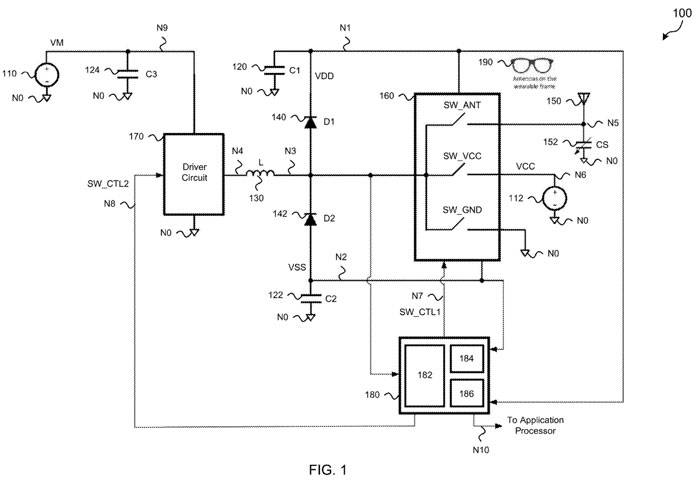
The first system 100 shown in Figure 1 uses a time-multiplexed resonant drive scheme to generate bipolar power in an LC resonant circuit and can be used in RF face detection applications. As shown in the figure, the system 100 includes a battery 110, a DC source 112, a first capacitor circuit 120, a second capacitor circuit 122, a third capacitor circuit 124, an inductor circuit 130, a first diode circuit 140, and a second diode. Circuit 142, antenna 150, sense capacitor 152, multiplexer MUX 160, driver circuit 170 and controller circuit 180. Antenna 150 may be positioned at various locations on the wearable MR device, such as wearable frame 190.
Battery 110 is coupled between node N9 and node NO to provide the corresponding battery voltage for the VM of node N9. DC source 112 is coupled between node N6 and node NO and provides voltage VCC at node N6. A first capacitive circuit 120 is coupled between node N1 and node NO, designated C1. The second capacitor circuit 122 is coupled between the node N2 and the node NO, which is set to C2. A third capacitive circuit 124 is coupled between node N9 and node NO, designated C3.
Inductor circuit 130 is coupled between node N3 and node N4, named l. A first diode circuit 140 is coupled between node N3 and node N1 and is designated D1. A second diode circuit 142 is coupled between node N2 and node N3, designated D2. Antenna 150 is coupled to node N5 and has a characteristic capacitance corresponding to sensing capacitor 152 .
Sensing capacitor 152 is coupled between node N5 and node NO, designated CS. MUX 160 includes an input port at node N3, a first output port at node N5, a second output port at node N6, a third output port at node NO, a first power port at node N1, a first power port at node N2 Second power port and control port at node N7.
The driving circuit 170 includes an output port of node N4, a first power port of node N9, a second power port of node NO, and a control port of node N8. Controller circuit 180 includes a first input port at node N1, a second input port at node N2, a third input port at node N3, a first output port at node N7, a second output port at node N8, and Third output port at node N10.
MUX 160 works together with the drive circuit 170 to effectively multiplex the charge and discharge time of the inductor circuit 130 at node N3 to the antenna 150 at node N7, the DC power supply 112 at node N6, or the circuit ground at node NO .
Detection capacitor 152 is represented as a capacitor having a variable capacitance value CS coupled between node N5 and node NO. Although shown as a physical capacitive component, sensing capacitance 152 corresponds to the characteristic capacitance of antenna 150 . Since the antenna is physically located on the wearable frame 900, the actual capacitance value of the antenna will vary based on proximity to the user's skin.
Inductive circuit 130 is effectively coupled in series between the output of driver circuit 170 and antenna 150 . From node N4 through inductor circuit 130 to sense capacitor 152, the LC filter circuit can be identified.
The controller circuit 180 may be implemented as a microcontroller unit MCU. The MCU can be configured through software or firmware instructions and controls the operation of circuit 100 according to a time division multiplexing scheme. The solution includes three basic modes: positive direction charging (first mode), negative direction charging (second mode), and operating the antenna as a sensor for facial motion detection (third mode).
In the first mode, the controller circuit 180 activates the first configuration of the drive circuit 170 through the second control signal SW_CTL2. The second control signal couples node N4 to node N9 such that node N4 effectively corresponds to battery voltage VM.
Also in this first mode, the controller circuit 180 pulses the first control signal SW_CTL1 to modulate the first switch configuration of the MUX 160 that selectively couples the node N3 through the third switch circuit in the MUX 160 Go to node NO. During the pulse high period, the circuit coupling node N3 to node NO is grounded, causing the inductor circuit 130 from node N4 to node N3 to charge in the positive direction.
During the pulse low period, node N3 is decoupled from node NO, and the storage current from the inductor circuit 130 flows through the first diode circuit 140, transferring the charge to the first capacitor circuit 120 (C1). Over time, the repeated pulses will cause an accumulation of charge on the first capacitor circuit 120 (C1) sufficient to produce a positive supply voltage VDD at node N1.
During the second mode, the controller circuit 180 activates the second driving configuration of the driving circuit 170 through the second control signal SW_CTL2. The control signal couples node N4 to node NO such that node N4 effectively corresponds to circuit ground.
In addition, in the second mode, the controller circuit 180 pulse modulates the second switch configuration for the MUX 160 through the first control signal SW_CTL1, and the switch selectively switches the MUX 160 through the second switch circuit in the MUX 160. Node N3 is coupled to node N6. During the pulse high period, node N3 is coupled to DC source 112 at node N6, causing inductor circuit 130 to charge in the negative direction from node N3 to node N4.
During the low period of the pulse, node N3 is decoupled from node N6, and the storage current from the inductor circuit 130 flows through the second diode circuit 140, providing charge to the second capacitor circuit 122 (C2). Over time, the repetitive pulses will cause an accumulation of charge on the second capacitor circuit 122 (C2) sufficient to produce a negative supply voltage VSS at node N2.
In the third mode, the controller circuit 180 selects the third switch configuration for the MUX 160 through the first control signal SW_CTL1. The switch couples node N3 to node N5 through a first switch circuit switch in MUX 160 .
Also in the third mode, the controller circuit 180 selectively activates the driving circuit 170 through the second control signal SW_CTL2. The second control signal pulses modulation node N4 coupled between node N9 and node NO. In this third mode, inductive circuit 130 is coupled to antenna 150 and its characteristic sensing capacitor 152 (CS), forming an LC resonant circuit.
By pulse modulating the coupling of node N4 between node N9 and node NO, the LC resonant circuit is excited to produce an observable oscillation signal at node N3, which can be used for face tracking. The dual supply voltages (VDD, VSS) previously generated in the first and second modes are used to operate various circuits, while the LC resonant circuit is excited in the third mode. Based on the high-Q resonance characteristics of the LC filter, the transient response will correspond to the AC signal at node N3.
Controller circuit 180 may be configured to capture the sensed signal from node N3, which may then be provided as a digital signal to node N10 to other systems for further processing. Due to the high-Q characteristics of the LC filter, the sensed signal may have significant peak-to-peak voltage. Therefore, additional circuitry may be required to scale down the signal size before being evaluated by controller circuit 180.
Figure 1 illustrates a dual-purpose inductor configuration used both to generate a DC voltage supply and as a DC-AC converter for RF facial motion detection, which is suitable for portable systems using battery power.
Microsoft notes that the proposed system includes an LC filter (or resonator) with a high quality factor, where the LC filter uses a series inductive circuit combined with a sensing capacitor formed by the user's sensing antenna and facial skin. . The LC filter is configured to amplify the AC voltage of the AC power source at the resonant frequency of the radio frequency facial tracking system.
An important aspect of the scheme described is that the facial tracking system benefits from reduced circuit complexity.
The resonant frequency of the LC filter changes as the antenna's sensing capacitance changes, which changes with facial movement relative to the antenna's position. For a given fixed input frequency, the gain and phase of the LC filter output signal will change as a function of the detected capacitance change. Due to the peak gain and high Q at the resonant frequency of the LC filter, a very large output signal can be achieved with a relatively small input signal.
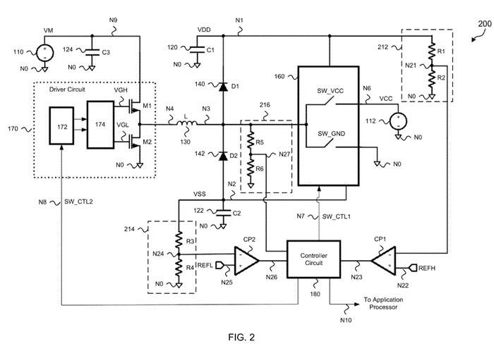
The second system 200 shown in Figure 2 uses a time-multiplexed resonant drive scheme to generate bipolar power in an LC resonant circuit and can be used in RF face detection applications. As shown in the figure, the system 200 includes a battery 110, a DC source 112, a first capacitor circuit 120, a second capacitor circuit 122, a third capacitor circuit 124, an inductor circuit 130, a first diode circuit 140, and a second diode. Circuit 142, multiplexer MUX 160, driver circuit 170 and controller circuit 180.
Compared with Figure 1, the system of Figure 2 includes two comparators CP1 and CP2, and three voltage dividers or scaling circuits (212, 214 and 216). The first voltage divider circuit 212 includes two resistors R1, R2 coupled in series between the node N1 and the node NO, and the output of the first voltage divider circuit corresponds to the node N21.
The first comparator CP1 includes an inverting input (−) coupled to node N21, a non-inverting input ( ) coupled to node N22, and an output coupled to node N23. The second voltage divider circuit 214 includes two resistors R3, R4 coupled in series between node N2 and node NO, the output of the second voltage divider circuit corresponding to node N24.
The second comparator CP2 includes an inverting input (−) coupled to node N24, a non-inverting input ( ) coupled to node N25, and an output coupled to node N26. The third voltage divider circuit 216 includes two resistors R5, R6 coupled in series between node N3 and node NO, the output of the second voltage divider circuit corresponding to node N27.
The voltage divider circuit described above is configured to reduce the voltage from a corresponding one of the input nodes to a suitable level for further processing. For example, a first voltage divider circuit consisting of resistors R1 and R2 detects the voltage at node N1 and produces a scaled version of the voltage detected at node N21.
Similarly, the second voltage divider circuit consisting of resistors R3 and R4 senses the voltage at node N2 and produces a scaled version of the sensed voltage at node N24; while the third voltage divider circuit consisting of resistors R5 and R6 The converter circuit senses the voltage at node N3 and generates a scaled version of the sensed voltage at node N27.
Comparators CP1 and CP2 are configured to detect when the corresponding voltage at their input reaches the target voltage. For example, the first comparator CP1 is configured to compare the sensing voltage of the node N21 with the first reference voltage REFH, and generate a signal at the node N23.
Similarly, configure the second comparator CP2 to compare the sensing voltage of node N24 with the second reference voltage REFL, and generate a signal at node N26.
Controller circuit 180 uses signals from nodes N23 and N26 as inputs to control the charging time and duty cycle of inductor circuit 130.
The output of third voltage divider circuit 216 is shown coupled to the input of controller circuit 180 at node N27. This input corresponds to a scaled version of the sensed voltage at node N3. In operation, the voltage at node N3 can represent the response of an LC resonant circuit, such as the LC resonant circuit composed of an inductor 130 and a sensing capacitor 152 as shown in FIG. 1 . The response of the LC resonant circuit measured at node N27 may be converted to a digital value by ADC 184 in controller circuit 180 .
The detailed implementation of the driving circuit 170 is also shown in Figure 2, which includes a logic block 172, a gate driving block 174, a field effect transistor M1 and a field effect transistor M2. Logic block 172 includes an input port coupled to node N8 and a pair of outputs coupled to gate driver block 174 . Gate driver block 177 includes a first output (VGH) coupled to the gate of FET M1 and a second output (VGL) coupled to the gate of FET M2.
FET M1 includes both a drain coupled to node N9 and a source coupled to node N4. FET M2 includes both a drain coupled to node N4 and a source coupled to node NO. Operationally, the signal at node N8 may represent a single control signal or multiple control signals that control the timing and duty cycle of charging of the inductor through drive circuit 170 .
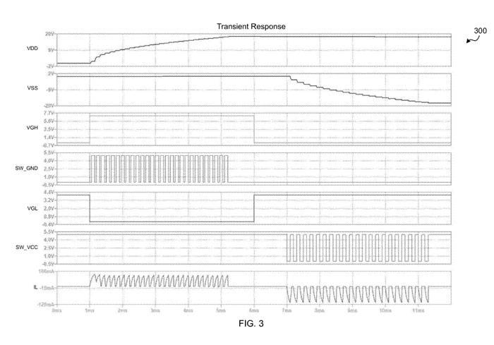
Figure 3 shows the transient response for an example time-multiplexed resonant drive scheme, such as the example system used for FIGS. 3 includes the voltage waveforms of the dual power supplies (VDD, VSS), the high and low gate control signals (VGH, VGL) of the driving circuit 170 , the first and second switch control signals of the multiplexing circuit 160 , and the flow in the inductor circuit 130 The current waveform of the current.
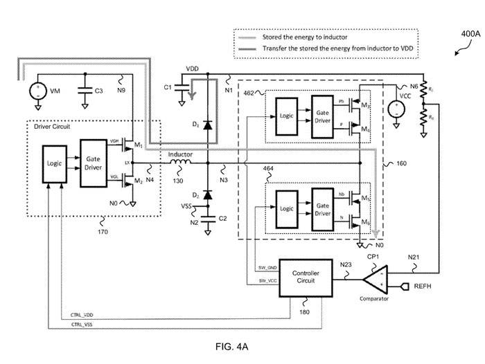
Figure 4A shows the first part of the operation of a third example time-multiplexed resonant drive scheme for generating bipolar power in an LC resonant circuit.
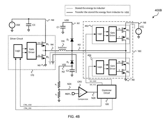
Figure 4B shows the second part of the operation of a third example time-multiplexed resonant drive scheme for generating bipolar power in an LC resonant circuit.
Figures 2, 4A and 4B show that the first field effect transistor and the second field effect transistor include n-type field effect transistors. Bipolar supplies (VDD, VSS) can be generated by operation of the driver circuit 170 as a half-bridge resonator, with two switches connected to a DC voltage source and ground by operation of a multiplexer.
Initially, capacitor C1 or C2 may not store charge, so the supply voltages VDD and VSS on nodes N1 and N2 may not meet requirements. Comparator CP1 compares the voltage of node N1 with the positive reference voltage REFH through the output of the first voltage divider (R1, R2) of node N21 and generates a comparator output at node N23.
Comparator CP2 (via the output of the second voltage divider (R3, R4) at node N24 compares the voltage at node N2 with the negative reference voltage REFL and produces a comparator output at node N26.
The controller circuit 180 evaluates the voltages of nodes N23 and N26, determines whether the voltage is not at the expected value, and generates one or more control signals to start the charging process of the power supply.
As shown in Figure 4A, when the power supply VDD at node N1 is too low, the high-side FET M2 of the half-bridge resonator is activated (such as VGH is high), and the low-side FET M2 is deactivated, thereby generating a positive power supply. The control signal is then used to control switching circuit 464 to circuit ground coupling node N3 of inductor circuit 130 to node NO.
When the switch circuit 464 is in the closed state, current flows from the battery VM through the drive circuit into the inductor circuit 130 at the node N4. The node N3 is coupled to the circuit ground at the node NO through the switch circuit 464. The inductor circuit 130 is effectively forward. Store current.
When the switch circuit 464 is in an open-circuit state, the energy stored in the current of the inductor circuit 130 flows to the node N1 through the diode circuit D1, and the capacitor C1 stores the charge in the node N1 and increases the power supply voltage VDD accordingly. Over multiple cycles of this modulation, the value of the positive supply VDD will increase until the desired positive voltage level is reached and comparator CP1 will trip to notify the controller circuit 180 that the desired level has been reached. Once the positive supply VDD reaches the desired value, the high-side switching FET M1 of the driver circuit 170 is deactivated by the controller circuit 180 .
As shown in Figure 4B, when the power VSS at node N2 is too high, the low-side FET M2 of the half-bridge resonator is activated, while the high-side FET M1 is deactivated, resulting in a negative power supply. The control signal is then used to modulate the switching circuit 462 to the DC source of node N3 to node N6 of the inductor circuit 130 or VCC.
When switch circuit 462 is in a closed state, current flows from DC source VCC at node N6 through inductor circuit 130 at node N3, where node N4 is coupled to circuit ground at node NO through drive circuit 170, and inductor circuit 130 effectively reverses to store current.
When the switch circuit 462 is in an open circuit state, the storage current in the inductor circuit 130 flows from the ground node NO, reaches the node N3 through the capacitor C2 and the diode circuit D1. In node N3, the energy of the inductor is transferred to capacitor C2, thereby reducing the supply voltage VSS.
Over multiple cycles of this modulation, the value of the negative supply VSS will decrease until the required negative voltage supply level is reached and comparator CP2 will trip to notify the controller circuit 180 that the required level has been reached. Once the negative supply VSS is at the desired value, the low-side switching FET M2 of the driver circuit 170 is deactivated by the controller circuit 180 .
Related Patents: Microsoft Patent | Time-multiplexing resonant drive scheme to generate dual polarity supplies
The Microsoft patent application titled "Time-multiplexing resonant drive scheme to generate dual polarity supplies" was originally submitted in December 2021 and was recently published by the US Patent and Trademark Office.
The above is the detailed content of Microsoft AR/VR patent proposes using time-multiplexed resonant drive to generate bipolar power supply. For more information, please follow other related articles on the PHP Chinese website!

Hot AI Tools

Undresser.AI Undress
AI-powered app for creating realistic nude photos

AI Clothes Remover
Online AI tool for removing clothes from photos.

Undress AI Tool
Undress images for free

Clothoff.io
AI clothes remover

AI Hentai Generator
Generate AI Hentai for free.

Hot Article

Hot Tools

Notepad++7.3.1
Easy-to-use and free code editor

SublimeText3 Chinese version
Chinese version, very easy to use

Zend Studio 13.0.1
Powerful PHP integrated development environment

Dreamweaver CS6
Visual web development tools

SublimeText3 Mac version
God-level code editing software (SublimeText3)

Hot Topics
 1376
1376
 52
52
 I Tried Vibe Coding with Cursor AI and It's Amazing!
Mar 20, 2025 pm 03:34 PM
Vibe coding is reshaping the world of software development by letting us create applications using natural language instead of endless lines of code. Inspired by visionaries like Andrej Karpathy, this innovative approach lets dev
 Top 5 GenAI Launches of February 2025: GPT-4.5, Grok-3 & More!
Mar 22, 2025 am 10:58 AM
February 2025 has been yet another game-changing month for generative AI, bringing us some of the most anticipated model upgrades and groundbreaking new features. From xAI’s Grok 3 and Anthropic’s Claude 3.7 Sonnet, to OpenAI’s G
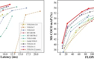 How to Use YOLO v12 for Object Detection?
Mar 22, 2025 am 11:07 AM
YOLO (You Only Look Once) has been a leading real-time object detection framework, with each iteration improving upon the previous versions. The latest version YOLO v12 introduces advancements that significantly enhance accuracy
 Is ChatGPT 4 O available?
Mar 28, 2025 pm 05:29 PM
ChatGPT 4 is currently available and widely used, demonstrating significant improvements in understanding context and generating coherent responses compared to its predecessors like ChatGPT 3.5. Future developments may include more personalized interactions and real-time data processing capabilities, further enhancing its potential for various applications.
 Google's GenCast: Weather Forecasting With GenCast Mini Demo
Mar 16, 2025 pm 01:46 PM
Google DeepMind's GenCast: A Revolutionary AI for Weather Forecasting Weather forecasting has undergone a dramatic transformation, moving from rudimentary observations to sophisticated AI-powered predictions. Google DeepMind's GenCast, a groundbreak
 Which AI is better than ChatGPT?
Mar 18, 2025 pm 06:05 PM
The article discusses AI models surpassing ChatGPT, like LaMDA, LLaMA, and Grok, highlighting their advantages in accuracy, understanding, and industry impact.(159 characters)
 o1 vs GPT-4o: Is OpenAI's New Model Better Than GPT-4o?
Mar 16, 2025 am 11:47 AM
OpenAI's o1: A 12-Day Gift Spree Begins with Their Most Powerful Model Yet December's arrival brings a global slowdown, snowflakes in some parts of the world, but OpenAI is just getting started. Sam Altman and his team are launching a 12-day gift ex
 Best AI Art Generators (Free & Paid) for Creative Projects
Apr 02, 2025 pm 06:10 PM
The article reviews top AI art generators, discussing their features, suitability for creative projects, and value. It highlights Midjourney as the best value for professionals and recommends DALL-E 2 for high-quality, customizable art.


