 Technology peripherals
 It Industry
 Samsung Electronics plans to launch dual-layer stack V-NAND flash memory technology with more than 300 layers next year
Samsung Electronics plans to launch dual-layer stack V-NAND flash memory technology with more than 300 layers next year
According to the latest reports, Samsung Electronics plans to launch 9th generation V-NAND flash memory products next year. This new product will use a dual-layer stack architecture with more than 300 layers, bringing a breakthrough in the field of storage technology
Samsung plans to introduce a dual-layer stack architecture to surpass the competition in terms of technological advancements Opponent SK Hynix. According to reports, SK Hynix plans to start mass production of 321-layer NAND flash memory with a three-layer stack architecture in the first half of 2025. However, as early as 2020, Samsung has successfully produced the 7th generation V-NAND flash memory chip
This innovative move is expected to significantly increase storage density, thereby helping to reduce the cost of solid-state drives manufacturing costs, providing consumers with more cost-effective storage solutions. Samsung's dual-layer stack architecture technology is a new stack built on the existing 3D NAND stack. This approach not only increases yields, but also uses resources more efficiently
According to the editor’s understanding, SK Hynix adopts a three-layer stack architecture that is different from its competitors. This architecture creates three different sets of layers on top of a 3D NAND layer. Although this can increase output, it will also increase the production steps and the use of raw materials. Industry insiders revealed to the Seoul Economic Daily that Samsung is launching the 9th generation 3D After NAND, it is expected to adopt a three-layer stack architecture in the 10th generation products, which is expected to reach 430 layers. This technology choice not only ensures higher throughput, but also copes with the raw material and cost pressures that may arise when exceeding 400 layers.
At the "2022 Samsung Technology Day" in 2022, Samsung proposed ambitious long-term goals, planning to bring 3D The number of NAND layers has been increased to 1,000. This goal shows Samsung's persistent pursuit of the development of future storage technology.
The above is the detailed content of Samsung Electronics plans to launch dual-layer stack V-NAND flash memory technology with more than 300 layers next year. For more information, please follow other related articles on the PHP Chinese website!

Hot AI Tools

Undresser.AI Undress
AI-powered app for creating realistic nude photos

AI Clothes Remover
Online AI tool for removing clothes from photos.

Undress AI Tool
Undress images for free

Clothoff.io
AI clothes remover

AI Hentai Generator
Generate AI Hentai for free.

Hot Article

Hot Tools

Notepad++7.3.1
Easy-to-use and free code editor

SublimeText3 Chinese version
Chinese version, very easy to use

Zend Studio 13.0.1
Powerful PHP integrated development environment

Dreamweaver CS6
Visual web development tools

SublimeText3 Mac version
God-level code editing software (SublimeText3)

Hot Topics
 Samsung to launch PM1753 data center-grade SSD: 14.8 GB/s sequential read, 3.4 million IOPS random read
Aug 08, 2024 pm 04:40 PM
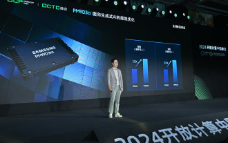
According to news from this site on August 8, Samsung demonstrated a variety of new SSD products at the 2024 Flash Memory Summit (FMS) - PM1753, BM1743, PM9D3a, PM9E1, and also tested the ninth generation QLCV-NAND, TLCV-NAND and CMM-D –DRAM, CMM-HTM, CMM-HPM, and CMM-BCXL technologies were introduced. BM1743 uses QLC flash memory with a capacity of up to 128TB, a continuous read speed of 7.5GB/s, a write speed of 3.5GB/s, a random read of 1.6 million IOPS, and a write of 45,000 IOPS. It adopts a 2.5-inch form factor and a U.2 interface, and is idle Power consumption is reduced to 4W, and after subsequent OTA updates, only
 Samsung Galaxy S25 Ultra mobile phone leaked: 6.86 inches, horizontal screen-to-body ratio 94.1%
Aug 17, 2024 pm 01:49 PM
According to news on August 17, the source @ibinguniverse posted on Weibo today, stating that the exact size of Apple iPhone 16 Pro Max is 6.88 inches, and the exact size of Galaxy S25 Ultra is 6.86 inches. Both can be regarded as 6.9 inches. Sources indicate that the Samsung Galaxy S25 Ultra has a narrower body and a wider screen than the S24 Ultra, with a horizontal screen-to-body ratio of 94.1%, while the S24 Ultra’s horizontal screen-to-body ratio is 91.5%. Fenye checked the relevant Weibo of the source. He also commented on the newly exposed photos of iPhone 16 Pro Max and believed that it was wrong to be close to a micro-curve. The phone is actually a straight screen + 2.5D glass.
 Samsung is revealed to start installing its first ASML High-NA EUV lithography machine by the end of 2024 at the earliest
Aug 16, 2024 am 11:11 AM
According to news from this site on August 16, the Seoul Economic Daily reported yesterday (August 15) that Samsung will install its first High-NAEUV lithography machine from ASML between the fourth quarter of 2024 and the first quarter of 2025. It is expected to be put into use in mid-2025. Reports indicate that Samsung will install the first ASMLTwinscanEXE:5000High-NA lithography machine in its Hwaseong campus, which will be mainly used for research and development purposes to develop next-generation manufacturing technologies for logic and DRAM. Samsung plans to develop a strong ecosystem around High-NAEUV technology: In addition to acquiring high-NAEUV lithography equipment, Samsung is also cooperating with Japan's Lasertec to develop high-NAEUV lithography equipment specifically for High-NAEUV lithography equipment.
 Samsung's 10,000-yuan foldable phone W25 revealed: 5-megapixel under-screen front camera and thinner body
Aug 23, 2024 pm 12:43 PM
According to news on August 23, Samsung is about to launch a new folding mobile phone W25, which is expected to be unveiled at the end of September. It will make corresponding improvements in the under-screen front camera and body thickness. According to reports, Samsung W25, codenamed Q6A, will be equipped with a 5-megapixel under-screen camera, which is an improvement over the 4-megapixel camera of the Galaxy Z Fold series. In addition, the W25’s external-screen front camera and ultra-wide-angle camera are expected to be 10 million and 12 million pixels respectively. In terms of design, the W25 is about 10 mm thick in the folded state, which is about 2 mm thinner than the standard Galaxy Z Fold 6. In terms of screen, the W25 has an external screen of 6.5 inches and an internal screen of 8 inches, while the Galaxy Z Fold6 has an external screen of 6.3 inches and an internal screen of 8 inches.
 Xiaomi 15 series full codenames revealed: Dada, Haotian, Xuanyuan
Aug 22, 2024 pm 06:47 PM
The Xiaomi Mi 15 series is expected to be officially released in October, and its full series codenames have been exposed in the foreign media MiCode code base. Among them, the flagship Xiaomi Mi 15 Ultra is codenamed "Xuanyuan" (meaning "Xuanyuan"). This name comes from the Yellow Emperor in Chinese mythology, which symbolizes nobility. Xiaomi 15 is codenamed "Dada", while Xiaomi 15Pro is named "Haotian" (meaning "Haotian"). The internal code name of Xiaomi Mi 15S Pro is "dijun", which alludes to Emperor Jun, the creator god of "The Classic of Mountains and Seas". Xiaomi 15Ultra series covers
 New evidence suggests Samsung Galaxy Z Flip6 phone supports New DeX mode
Jul 27, 2024 pm 06:06 PM
According to news on July 27, technology media Android Authority published a correction blog post today (July 27), stating that Samsung Galaxy Z Flip 6 mobile phone supports DeX, but it is not the version that many users are accustomed to. NewDeX and ClassicDeX Note: In the OneUI6 system released by Samsung last year, the DeX interface for tablet devices was improved and "NewDeX" was introduced. The original DeX is now renamed "ClassicDeX" and users can switch according to their preferences. fenye "NewDeX" main changes cancel the status bar and navigation bar merger, remove some display zoom and attachment settings NewDeX advantages startup speed improvement adopt OneUIHome launcher
 A first look at the Samsung Galaxy Z Fold6 / Flip6 mobile phone Gemini Nano AI model: running locally, not yet integrated into Galaxy AI
Aug 10, 2024 pm 01:59 PM
According to news on August 10, technology media Android Authority published a blog post on August 8, stating that Samsung Galaxy Z Fold6 and Galaxy Z Flip 6 have become the first folding phones to support local running of the Gemini Nano AI model. It has not yet been integrated into Galaxy AI. According to reports citing sources, the Galaxy AI and Gemini Nano AI models are two independent systems at this stage. The two have not yet been integrated. Even text-based functions (such as chat assistance, note assistance, text recording assistance or browsing assistance) ) neither. This media test can run GalaxyAI locally without downloading the GeminiNano model: Samsun
 Samsung will provide displays for Microsoft's MR headsets, and the devices are expected to be lighter and have clearer displays
Aug 10, 2024 pm 09:45 PM
Recently, Samsung Display and Microsoft signed an important cooperation agreement. According to the agreement, Samsung Display will develop and supply hundreds of thousands of OLEDoS panels for mixed reality (MR) head-mounted devices to Microsoft. Microsoft is developing an MR device for multimedia content such as games and movies. This device is expected to It will be launched after the OLEDoS specifications are finalized, mainly serving the commercial field, and is expected to be delivered as early as 2026. OLEDoS (OLED on Silicon) technology OLEDoS is a new display technology that deposits OLED on a silicon substrate. Compared with traditional glass substrates, it is thinner and has higher pixels. OLEDoS display and ordinary display


