 Technology peripherals
 It Industry
 Samsung plans to mass-produce ninth-generation V-NAND flash memory with more than 300 layers early next year, claiming to have the highest number of layers in the industry
Samsung plans to mass-produce ninth-generation V-NAND flash memory with more than 300 layers early next year, claiming to have the highest number of layers in the industry
According to news from this site on October 19, Samsung is the world’s largest NAND flash memory supplier and has ambitious plans for the development of V-NAND (what Samsung calls 3D NAND). This week Samsung shared some relevant information. information. The company confirmed that it is on track to produce its ninth-generation V-NAND flash memory with more than 300 layers, saying it will be the most layer-count 3D NAND in the industry.
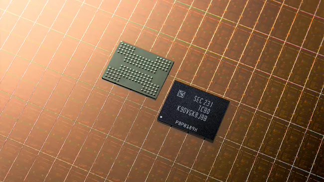
“The ninth-generation V-NAND is based on a double-layer structure, with the number of layers reaching the highest level in the industry, and will begin mass production early next year. Lee Jung-Bae, president of Samsung Electronics and head of its memory division, wrote in a blog post.
This site noticed that in August there was news that Samsung was developing a ninth-generation V-NAND with more than 300 layers and would continue to use the double-layer technology first used by Samsung in 2020. And Samsung now says its 3D NAND will have more effective layers than its competitors. We currently know that SK Hynix’s next-generation 3D NAND will have 321 layers, so Samsung’s ninth-generation V-NAND should have even more layers.
The increase in layer count will allow Samsung to increase the storage density of its 3D NAND devices. The company expects that future flash memory types will not only increase storage density but also improve performance.
"Samsung is also working on next-generation value-creating technologies, including a new structure that can maximize the input/output (I/O) speed of V-NAND." Lee Jung-bae said.
It’s not yet known how Samsung’s ninth-generation V-NAND will perform in terms of performance, but it is believed that the company will use this memory to produce its upcoming solid-state drives, possibly using the PCIe Gen5 interface .
As for longer-term technology innovation, Samsung is committed to minimizing cell interference, reducing height and maximizing the number of vertical layers, which will enable it to achieve the smallest cell size in the industry. These innovations will play a key role in advancing Samsung's vision of 3D NAND with over 1,000 layers and highly differentiated memory solutions.
Advertising statement: The external jump links (including but not limited to hyperlinks, QR codes, passwords, etc.) contained in the article are used to convey more information and save selection time. The results are for reference only. All articles on the site contain this statement.
The above is the detailed content of Samsung plans to mass-produce ninth-generation V-NAND flash memory with more than 300 layers early next year, claiming to have the highest number of layers in the industry. For more information, please follow other related articles on the PHP Chinese website!

Hot AI Tools

Undresser.AI Undress
AI-powered app for creating realistic nude photos

AI Clothes Remover
Online AI tool for removing clothes from photos.

Undress AI Tool
Undress images for free

Clothoff.io
AI clothes remover

AI Hentai Generator
Generate AI Hentai for free.

Hot Article

Hot Tools

Notepad++7.3.1
Easy-to-use and free code editor

SublimeText3 Chinese version
Chinese version, very easy to use

Zend Studio 13.0.1
Powerful PHP integrated development environment

Dreamweaver CS6
Visual web development tools

SublimeText3 Mac version
God-level code editing software (SublimeText3)

Hot Topics
 Samsung to launch PM1753 data center-grade SSD: 14.8 GB/s sequential read, 3.4 million IOPS random read
Aug 08, 2024 pm 04:40 PM
According to news from this site on August 8, Samsung demonstrated a variety of new SSD products at the 2024 Flash Memory Summit (FMS) - PM1753, BM1743, PM9D3a, PM9E1, and also tested the ninth generation QLCV-NAND, TLCV-NAND and CMM-D –DRAM, CMM-HTM, CMM-HPM, and CMM-BCXL technologies were introduced. BM1743 uses QLC flash memory with a capacity of up to 128TB, a continuous read speed of 7.5GB/s, a write speed of 3.5GB/s, a random read of 1.6 million IOPS, and a write of 45,000 IOPS. It adopts a 2.5-inch form factor and a U.2 interface, and is idle Power consumption is reduced to 4W, and after subsequent OTA updates, only
 Industry's highest transfer rate of 3.6GB/s, Micron announces mass production of ninth-generation 276-layer TLC NAND flash memory
Jul 31, 2024 am 08:05 AM
According to news from this site on July 30, Micron announced today (local time) that its ninth generation (site note: 276 layers) 3DTLC NAND flash memory will be mass-produced and shipped. Micron said that its G9NAND has the industry's highest I/O transfer rate of 3.6GB/s (i.e. 3600MT/s flash memory interface rate), which is 50% higher than the existing competing products of 2400MT/s, and can better meet the needs of data-intensive workloads. High throughput requirements. At the same time, Micron's G9NAND is 99% and 88% higher than other solutions on the market in terms of write bandwidth and read bandwidth respectively. This NAND particle-level advantage will bring performance and energy efficiency to solid-state drives and embedded storage solutions. improvement. In addition, like previous generations of Micron NAND flash memory, Micron 276
 Samsung Galaxy S25 Ultra mobile phone leaked: 6.86 inches, horizontal screen-to-body ratio 94.1%
Aug 17, 2024 pm 01:49 PM
According to news on August 17, the source @ibinguniverse posted on Weibo today, stating that the exact size of Apple iPhone 16 Pro Max is 6.88 inches, and the exact size of Galaxy S25 Ultra is 6.86 inches. Both can be regarded as 6.9 inches. Sources indicate that the Samsung Galaxy S25 Ultra has a narrower body and a wider screen than the S24 Ultra, with a horizontal screen-to-body ratio of 94.1%, while the S24 Ultra’s horizontal screen-to-body ratio is 91.5%. Fenye checked the relevant Weibo of the source. He also commented on the newly exposed photos of iPhone 16 Pro Max and believed that it was wrong to be close to a micro-curve. The phone is actually a straight screen + 2.5D glass.
 Samsung is revealed to start installing its first ASML High-NA EUV lithography machine by the end of 2024 at the earliest
Aug 16, 2024 am 11:11 AM
According to news from this site on August 16, the Seoul Economic Daily reported yesterday (August 15) that Samsung will install its first High-NAEUV lithography machine from ASML between the fourth quarter of 2024 and the first quarter of 2025. It is expected to be put into use in mid-2025. Reports indicate that Samsung will install the first ASMLTwinscanEXE:5000High-NA lithography machine in its Hwaseong campus, which will be mainly used for research and development purposes to develop next-generation manufacturing technologies for logic and DRAM. Samsung plans to develop a strong ecosystem around High-NAEUV technology: In addition to acquiring high-NAEUV lithography equipment, Samsung is also cooperating with Japan's Lasertec to develop high-NAEUV lithography equipment specifically for High-NAEUV lithography equipment.
 Samsung's 10,000-yuan foldable phone W25 revealed: 5-megapixel under-screen front camera and thinner body
Aug 23, 2024 pm 12:43 PM
According to news on August 23, Samsung is about to launch a new folding mobile phone W25, which is expected to be unveiled at the end of September. It will make corresponding improvements in the under-screen front camera and body thickness. According to reports, Samsung W25, codenamed Q6A, will be equipped with a 5-megapixel under-screen camera, which is an improvement over the 4-megapixel camera of the Galaxy Z Fold series. In addition, the W25’s external-screen front camera and ultra-wide-angle camera are expected to be 10 million and 12 million pixels respectively. In terms of design, the W25 is about 10 mm thick in the folded state, which is about 2 mm thinner than the standard Galaxy Z Fold 6. In terms of screen, the W25 has an external screen of 6.5 inches and an internal screen of 8 inches, while the Galaxy Z Fold6 has an external screen of 6.3 inches and an internal screen of 8 inches.
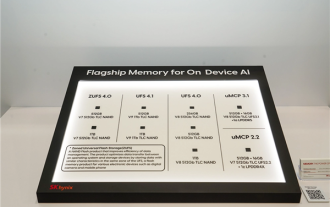 Hynix is the first to demonstrate UFS 4.1 flash memory: based on V9 TLC NAND particles
Aug 09, 2024 pm 03:33 PM
According to news on August 9, at the FMS2024 Summit, SK Hynix demonstrated its latest storage products, including UFS4.1 universal flash memory that has not yet officially released specifications. According to the official website of the JEDEC Solid State Technology Association, the latest UFS specification currently announced is UFS4.0 in August 2022. Its theoretical interface speed is as high as 46.4Gbps. It is expected that UFS4.1 will further improve the transmission rate. 1. Hynix demonstrated 512GB and 1TBUFS4.1 general-purpose flash memory products, based on 321-layer V91TbTLCNAND flash memory. SK Hynix also exhibited 3.2GbpsV92TbQLC and 3.6GbpsV9H1TbTLC particles. Hynix shows off V7-based
 Xiaomi 15 series full codenames revealed: Dada, Haotian, Xuanyuan
Aug 22, 2024 pm 06:47 PM
The Xiaomi Mi 15 series is expected to be officially released in October, and its full series codenames have been exposed in the foreign media MiCode code base. Among them, the flagship Xiaomi Mi 15 Ultra is codenamed "Xuanyuan" (meaning "Xuanyuan"). This name comes from the Yellow Emperor in Chinese mythology, which symbolizes nobility. Xiaomi 15 is codenamed "Dada", while Xiaomi 15Pro is named "Haotian" (meaning "Haotian"). The internal code name of Xiaomi Mi 15S Pro is "dijun", which alludes to Emperor Jun, the creator god of "The Classic of Mountains and Seas". Xiaomi 15Ultra series covers
 SK Hynix takes the lead in demonstrating UFS 4.1 universal flash memory, based on V9 TLC NAND particles
Aug 09, 2024 am 10:42 AM
According to news from this website on August 9, according to a press release issued by SK Hynix yesterday local time, the company demonstrated a series of new storage products at the FMS2024 Summit, including USF4.1 universal flash memory that has not yet officially released specifications. According to the official website of the JEDEC Solid State Technology Association, the latest UFS specification currently announced is UFS4.0 in August 2022. UFS4.0 specifies a theoretical interface speed of up to 46.4Gbps for each device, and USF4.1 is expected to further improve the transmission rate. ▲JEDECUFS specification page SK Hynix demonstrated two UFS4.1 general-purpose flash memories with capacities of 512GB and 1TB respectively, both based on the 321-layer stacked V91TbTLCNAND flash memory.


