 Technology peripherals
 AI
AI
 Microsoft patent proposes improved sensor capacitance measurement for AR glasses facial tracking
Microsoft patent proposes improved sensor capacitance measurement for AR glasses facial tracking
(Nweon January 4, 2024) Head-mounted devices can include facial tracking sensors for tracking facial movement. One way to perform face tracking is to use an array of face tracking sensors to measure capacitance values. When facial muscles move, the capacitance of the facial tracking sensor changes depending on the proximity of the facial surface to the corresponding sensor.
One possible way to determine the capacitance is to use a resonant LC circuit containing the sensing capacitance of the face tracking sensor. Changing the surface proximity to the sensing capacitor can cause a measurable change in the resonant frequency of the resonant LC circuit. However, capacitive crosstalk can occur between the array's face-tracking sensors, complicating simultaneous capacitance measurements from multiple sensors.
In the patent application titled "Determining charge on a facial-tracking sensor," Microsoft describes a method that determines the capacitance of the facial-tracking sensor's sensory capacitor by determining the amount of charge stored in the electrode of the sensory capacitor.
Briefly stated, a face tracking sensor includes sensing capacitor electrodes configured to be positioned proximate the surface of the face. The inductive capacitor electrode forms a capacitance based on the distance between the inductive capacitor electrode and the surface. The controller applies a reference voltage to the inductive capacitance electrode of the face tracking sensor.
The charge sensing circuit then determines the capacitance on the sensing capacitor electrode by determining the amount of charge accumulated on the sensing capacitor electrode due to the application of the reference voltage.
In one embodiment, the controller applies a reference voltage to the shielding track simultaneously along the electrical connection between the charge sensing circuit and the face tracking sensor. The reference voltage of the shielding track helps reduce capacitive crosstalk received by the face tracking sensor.
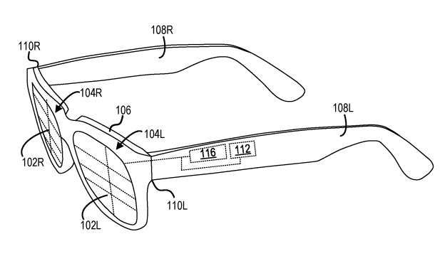
Figure 1 shows an example head mounted device 100 including multiple face tracking sensors. Specifically, the head mounted device 100 includes a left capacitive electrode array 102L formed on the left lens 104L of the head mounted device 100 and a right capacitive electrode array 102R formed on the right lens 104R.
Each of the left sense capacitor electrode array 102L and the right sense capacitor electrode array 102R includes a plurality of sense capacitor electrodes, each sense capacitor electrode configured to sense a different area of the wearer's face. Each sensing capacitor electrode is configured to be positioned proximate the surface of the person's face and form a capacitance based on the distance between the sensing capacitor electrode and the surface of the person's face.
Sensing capacitor electrode arrays 102L, 102R are formed from an at least partially optically transparent conductive film. The film may include one or more conductive materials, such as indium tin oxide, graphene, or other suitable materials. The thin film can be formed by any suitable process, such as chemical vapor deposition. The trench formed between the sensing capacitor electrodes can be used to place conductive traces. Because conductive films are not completely optically transparent, using relatively thin films for sensing capacitor electrodes can provide greater transparency than relatively thick coatings.
The head mounted device 100 includes multiple charge sensing circuits at the same time, as shown in Figure 112. Each of the plurality of charge sensing circuits 112 is connected to a corresponding face tracking sensor. Each charge sensing circuit 112 is configured to determine the capacitance of a corresponding sensing capacitor electrode by determining the amount of charge accumulated on the corresponding sensing capacitor electrode as a result of application of a reference voltage.
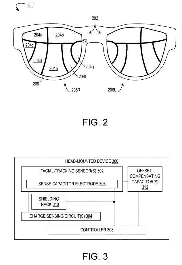
Figure 2 shows an example layout 202 of a sensing capacitor electrode array including a plurality of sensing capacitor electrodes. As shown, sense capacitor electrodes 204a-g are separated by trench regions 208, represented by thick black lines. Trench region 208 is a region between sense capacitor electrodes lacking the conductive film forming sense capacitor electrodes 204a-g. Trench region 208 may include conductive traces to connect sensing capacitor electrodes 204a-g to charge sensing circuitry and/or other circuitry.
Layout 202 is visible in the particular example because the conductive film forming the array of sensing capacitor electrodes is not completely transparent. However, when incorporated into a head-mounted device configuration, layout 202 may be positioned closer than the focal length of the human eye during most normal use. Therefore layout 202 can be out of focus for the user during ordinary device use and therefore not obstruct or distract the user.
Figure 3 shows an example head mounted device 300. Head mounted device 300 includes one or more face tracking sensors 302, and corresponding one or more charge sensing circuits 304. Each face tracking sensor 302 includes a sensory capacitor electrode 306 configured to be positioned proximate the facial surface, which can form a capacitance based on the distance between the sensory capacitor electrode 306 and the facial surface.
The head mounted device 300 also includes a controller 308 configured to apply a reference voltage to the sensing capacitor electrodes 306 of the one or more face tracking sensors 302 .
As described above, each charge sensing circuit 304 is configured to determine the amount of charge generated by the reference voltage and accumulated on the sensing capacitor electrode 306 to determine the sensing capacitor electrode 306 of the corresponding face tracking sensor 302 capacitance. For example, capacitance C can be determined as Q=C*V, where V is the reference voltage and Q is the amount of charge accumulated on the sensing capacitor electrode 306 resulting from the reference voltage.
In one embodiment, each charge sensing circuit 304 is further configured to generate a plurality of capacitances based at least on oversampling the amount of charge accumulated in the sensing capacitor electrode 306 of the corresponding face tracking sensor 302 generated by the reference voltage. place value. Oversampling involves resampling the charge of the sensor capacitor electrode 306 and filtering the resampled samples.
In one embodiment, the charge accumulated in each of multiple sensing capacitor electrodes 306 may be determined simultaneously. Accordingly, the controller 308 may be configured to operate one or more of the respective charge sensing circuits 304 concurrently. Such a configuration may facilitate faster operation than a configuration that utilizes time-multiplexed operation of the face tracking sensor.
The headset 300 also includes a shielding track 310 along electrical connections between one or more charge sensing circuits 304 and corresponding one or more face tracking sensors 302 . Shielding track 310 may help reduce electrical interference from conductors proximate the electrical connection between one or more face tracking sensors 302 and the corresponding charge sensing circuit(s) 304 , such as capacitive crosstalk between sensing capacitor electrodes 306 .
Reducing capacitive crosstalk can help reduce sensing errors and/or reduce noise. For example, shielding track 310 may help electrically cancel stray capacitance between the electrical ground and electrical connections of headset 300 .
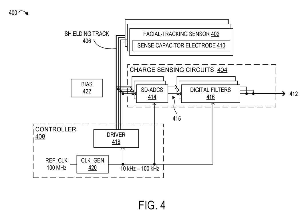
Figure 4 depicts a more detailed block diagram of head mounted device 400. Head mounted device 400 is an example implementation of head mounted device 300 . Similar to head mounted device 300, head mounted device 400 includes a plurality of face tracking sensors 402, a corresponding plurality of charge sensing circuits 404, a shielding track 406, and a controller 408.
Similar to face tracking sensor 302 , each face tracking sensor of plurality of face tracking sensors 402 includes a sensing capacitor electrode 410 . In the depicted embodiment, each charge sensing circuit 404 is configured to generate a plurality of capacitance bit values 412 based at least on oversampling the amount of accumulated charge. Each charge sensing circuit 404 includes an SD-ADC 414 and a digital filter 416 connected to the output of the SD-ADC 414 .
As an example, SD-ADC 414 oversamples the input of charge sensing circuit 404 and outputs bit stream 415. The bitstream indicates the amount of accumulated charge based at least on oversampling the input.
In one embodiment, oversampling may include an oversampling ratio in the range of 50 to 256. In other embodiments, oversampling may include any other suitable oversampling ratio. Input oversampling may help improve the accuracy of the SD-ADC 414, allow noise shaping of analog-to-digital conversion, and/or reduce the design complexity of the SD-ADC 414. As an example, noise shaping can shape noise to higher frequencies and thus facilitate filtering of noise.
The digital filter 416 converts the bit stream 415 from the SD-ADC 414 into the plurality of capacitance bit values 412 and filters the high frequency noise from the plurality of capacitance bit values 412. This noise filtering helps improve the signal-to-noise ratio. In the example where SD-ADC 414 includes a second-order SD-ADC, digital filter 416 includes a second-order filter. In other examples, each SD-ADC 414 and each digital filter 416 may include any suitable order of SD-ADCs and digital filters, respectively.
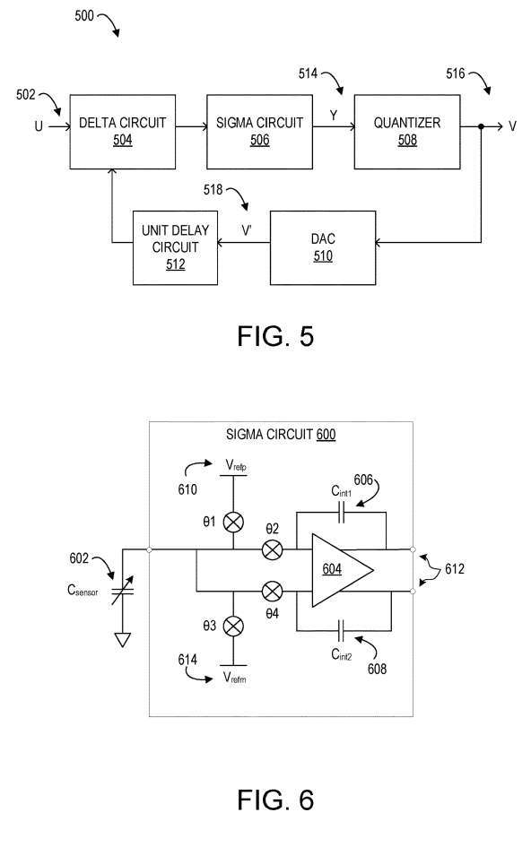
Figure 5 depicts a block diagram of an example SD-ADC 500. SD-ADC 500 is an example implementation of SD-ADC 414. SD-ADC 500 receives an analog input U 502 and outputs a digital output V through increment circuit 504 , Sigma circuit 506 and quantizer 508 .
SD-ADC 500 also includes a feedback path including digital-to-analog converter DAC 510 and unit delay circuit 512. Delta circuit 504 compares the difference between input U 502 and the feedback path output. For example, delta circuit 504 may compare the analog voltage difference between input U 502 and the feedback path output.
Next, Sigma circuit 506 is configured to output node y514, based at least on the average of the output of Delta circuit 504 over time. The average over time can be determined in continuous time or discrete time. Sigma circuit 506 may include an integrator circuit as described below and/or any other suitable circuit.
Next, the quantizer 508 samples the node y514 and outputs a digital value based on the sampled value of the node y514 to form a bit stream 516. As a specific example, quantizer 508 may include a comparator circuit configured to output a logic 0 or logic 1 on one clock cycle when node y 514 is below or above the quantizer reference voltage, respectively.
Figure 6 shows an example Sigma circuit 600 connected to a sense capacitor electrode 602. For example, SD-ADC 414 and SD-ADC 500 may use Sigma circuit 600. Sigma circuit 600 includes an integrator 604 having a first integrator capacitor 606 and a second integrator capacitor 608 . The operation of the sigma circuit 600 is controlled by the first control point θ1, the second control point θ2, the third control point θ3, and the fourth control point θ4. In some examples, a controller external to Sigma circuit 600 (eg, controller 408) may control the first, second, third, and fourth control points.
When the first control point θ1 is conductive, the first reference voltage 610 is connected to the sensing capacitor electrode 602. In this manner, a first reference voltage 610 is applied to the sensing capacitor electrode 602. Then, the first control point θ1 is turned on, the second control point θ2 is turned on, and the charge generated by the reference voltage and accumulated in the sensing capacitor electrode 602 is transferred to the first integrator capacitor 606 . The first integrator capacitor 606 and the integrator 604 output a voltage based on the accumulated charge.
In another embodiment, when the first control point θ1 is turned on, the second control point θ2 and the fourth control point θ4 are turned on, transferring the charge accumulated on the sensing capacitor electrode 602 to the first integrator capacitor 606 and second integrator capacitor 608.
In such a configuration, the integrator 604 is fully differentiated and the accumulated charge is divided between the first and second integrator capacitors 606, 608. Therefore, the output voltage is split between the output nodes of integrator 604, as shown at 612. A fully differential integrator can help improve the accuracy of the SD-ADC, reduce sensitivity to spurious noise and/or coupling, and/or reduce the design complexity of the SD-ADC.
Next, when the third control point θ3 is turned on, the second reference voltage 614 is connected and applied to the sensing capacitor electrode 602. In the depicted embodiment, applying a first reference voltage 610 during the first cycle directs the charge accumulated at the sensing capacitor electrode 602 to the non-inverting input of the integrator 604, and applying a second reference voltage 614 during the second cycle The charge accumulated at the sense capacitor electrode 602 is directed to the inverting input of the integrator 604 .
Similarly, the third control point θ3 is turned on, and the fourth control point θ4 is turned on, transferring the charge accumulated on the sensing capacitor electrode 602 to the second integrator capacitor 608. The second integrator capacitor 608 and the integrator 604 then output a voltage based on the accumulated charge. In other embodiments, the first, second, third and fourth control points may be controlled in any other suitable manner.
In one embodiment, one or more face tracking sensors of a device may electrically see a bias capacitance that is greater than the capacitance to a near point on the face, which may interfere with sensing of the smaller capacitance of the face. . This offset capacitance can be electrically offset by using a capacitor with a similar or equivalent capacitance value to the offset capacitance.
However, larger capacitors may consume more area. Therefore, the headset 700 shown in FIG. 7 utilizes a relatively small fixed capacitor 702 that can be connected to the sense capacitor electrode 704 to electrically cancel the bias capacitance 706 .
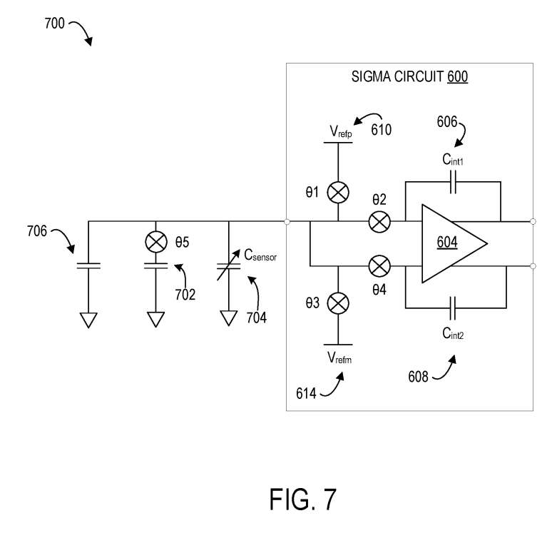
In the depicted example, as mentioned above, the first control point θ1 is turned on and the first reference voltage 610 is applied to the sensing capacitor electrode 704 . Then, the first control point θ1 is opened and the fifth control point θ5 located on the fixed capacitor 702 connection is toggled to electrically cancel the bias capacitance 706 on the sensing capacitor electrode 704 . The number of switches may be based on the capacitance value of fixed capacitor 702 and the value of bias capacitor 706 .
For example, when the bias capacitor 706 is 10 times larger than the fixed capacitor 702, the fifth control point θ5 can be switched 10 times to electrically offset the bias capacitor 706. Switching using the fifth control point θ5 can help reduce the size of the fixed capacitor 702 on the headset 700 compared to an implementation that omits such switching. Figure 7 shows a single sensing capacitor electrode, fixed capacitor and sigma circuit, other embodiments may include multiple sensing capacitor electrodes and corresponding multiple fixed capacitors and sigma circuits.
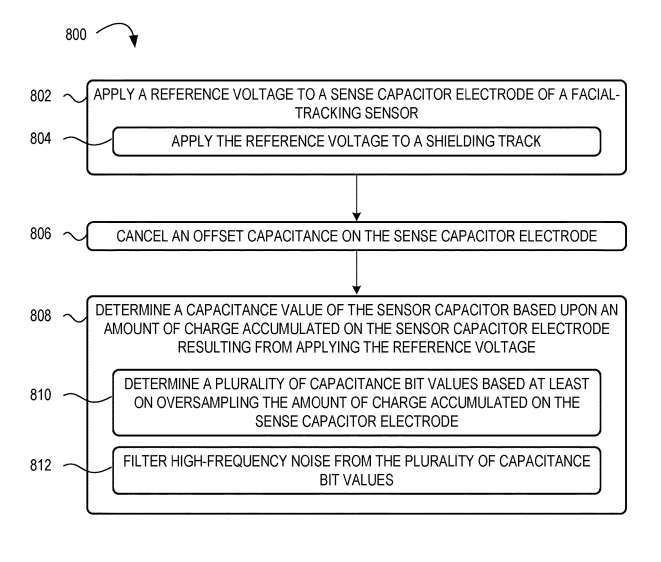
Figure 8 depicts a flowchart of an example method 800 for determining a sense capacitor electrode capacitance value.
At 802, a reference voltage is applied to the sensing capacitance electrode of the face tracking sensor.
At 804, a reference voltage is applied to the shielding track along the electrical connection between the face tracking sensor and the charge sensing circuit. Applying a reference voltage to the shielded track can help electrically cancel the capacitance between the sensing capacitor electrodes of multiple face tracking sensors on the headset. Additionally, applying the reference voltage to the shield trace may help enable simultaneous operation of corresponding multiple charge sensing circuits.
As mentioned above, the headset can see offset capacitance at the sensing capacitor electrodes. In such an example, 806 includes discharging the offset capacitance by switching the connections of the offset compensation capacitor, thereby eliminating the offset capacitance on the sensing capacitor electrodes.
In one embodiment, the offset compensation capacitor may include a smaller fixed capacitor that can be switched multiple times. In this way, the smaller fixed capacitance electrically cancels out the larger bias capacitance. In other examples, the offset compensation capacitor may include a programmable capacitor that is selectively controllable to adjust the capacitance value.
Continuing at 808, a capacitance value of the sensing capacitor electrode of the face tracking sensor is determined based on the amount of charge accumulated at the sensing capacitor electrode of the face tracking sensor due to the application of the reference voltage.
In one embodiment, determining the capacitance value of the sensing capacitor electrode includes determining a plurality of capacitance bit values based on at least oversampling an amount of charge accumulated by the sensing capacitor electrode of the face tracking sensor, As shown in 810.
As an example, the plurality of capacitance bit values may include a binary number indicating the amount of charge accumulated on the sensing capacitor electrode. As mentioned earlier, SD-ADCs can shape noise at multiple capacitor values to higher frequencies. Accordingly, method 800 includes filtering out high frequency noise from the plurality of capacitance bit values at 812 . Filtering high-frequency noise helps improve the signal-to-noise ratio of the capacitor bit value.
Related Patents: Microsoft Patent | Determining charge on a facial-tracking sensor
The Microsoft patent application titled "Determining charge on a facial-tracking sensor" was originally submitted in June 2022 and was recently published by the US Patent and Trademark Office.
It should be noted that, generally speaking, after a U.S. patent application is reviewed, it will be automatically published 18 months from the filing date or priority date, or it will be published within 18 months from the filing date at the request of the applicant. Note that publication of a patent application does not mean that the patent is approved. After a patent application is filed, the USPTO requires actual review, which can take anywhere from 1 to 3 years.
In addition, this is just a patent application, which does not mean it will be approved. At the same time, it is not sure whether it will be actually commercialized and the actual application effect.
The above is the detailed content of Microsoft patent proposes improved sensor capacitance measurement for AR glasses facial tracking. For more information, please follow other related articles on the PHP Chinese website!

Hot AI Tools

Undresser.AI Undress
AI-powered app for creating realistic nude photos

AI Clothes Remover
Online AI tool for removing clothes from photos.

Undress AI Tool
Undress images for free

Clothoff.io
AI clothes remover

AI Hentai Generator
Generate AI Hentai for free.

Hot Article

Hot Tools

Notepad++7.3.1
Easy-to-use and free code editor

SublimeText3 Chinese version
Chinese version, very easy to use

Zend Studio 13.0.1
Powerful PHP integrated development environment

Dreamweaver CS6
Visual web development tools

SublimeText3 Mac version
God-level code editing software (SublimeText3)

Hot Topics
 I Tried Vibe Coding with Cursor AI and It's Amazing!
Mar 20, 2025 pm 03:34 PM
Vibe coding is reshaping the world of software development by letting us create applications using natural language instead of endless lines of code. Inspired by visionaries like Andrej Karpathy, this innovative approach lets dev
 How to Use DALL-E 3: Tips, Examples, and Features
Mar 09, 2025 pm 01:00 PM
DALL-E 3: A Generative AI Image Creation Tool Generative AI is revolutionizing content creation, and DALL-E 3, OpenAI's latest image generation model, is at the forefront. Released in October 2023, it builds upon its predecessors, DALL-E and DALL-E 2
 Top 5 GenAI Launches of February 2025: GPT-4.5, Grok-3 & More!
Mar 22, 2025 am 10:58 AM
February 2025 has been yet another game-changing month for generative AI, bringing us some of the most anticipated model upgrades and groundbreaking new features. From xAI’s Grok 3 and Anthropic’s Claude 3.7 Sonnet, to OpenAI’s G
 How to Use YOLO v12 for Object Detection?
Mar 22, 2025 am 11:07 AM
YOLO (You Only Look Once) has been a leading real-time object detection framework, with each iteration improving upon the previous versions. The latest version YOLO v12 introduces advancements that significantly enhance accuracy
 Elon Musk & Sam Altman Clash over $500 Billion Stargate Project
Mar 08, 2025 am 11:15 AM
The $500 billion Stargate AI project, backed by tech giants like OpenAI, SoftBank, Oracle, and Nvidia, and supported by the U.S. government, aims to solidify American AI leadership. This ambitious undertaking promises a future shaped by AI advanceme
 Sora vs Veo 2: Which One Creates More Realistic Videos?
Mar 10, 2025 pm 12:22 PM
Google's Veo 2 and OpenAI's Sora: Which AI video generator reigns supreme? Both platforms generate impressive AI videos, but their strengths lie in different areas. This comparison, using various prompts, reveals which tool best suits your needs. T
 Google's GenCast: Weather Forecasting With GenCast Mini Demo
Mar 16, 2025 pm 01:46 PM
Google DeepMind's GenCast: A Revolutionary AI for Weather Forecasting Weather forecasting has undergone a dramatic transformation, moving from rudimentary observations to sophisticated AI-powered predictions. Google DeepMind's GenCast, a groundbreak
 Which AI is better than ChatGPT?
Mar 18, 2025 pm 06:05 PM
The article discusses AI models surpassing ChatGPT, like LaMDA, LLaMA, and Grok, highlighting their advantages in accuracy, understanding, and industry impact.(159 characters)


