
 Technology peripherals
It Industry
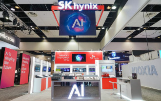
SK Hynix plans to accelerate the development of HBM4 and commercialize CXL memory to start mass production in 2024
Technology peripherals
It Industry
SK Hynix plans to accelerate the development of HBM4 and commercialize CXL memory to start mass production in 2024
SK Hynix plans to accelerate the development of HBM4 and commercialize CXL memory to start mass production in 2024

SK Hynix released its annual AI memory summary on this site on December 24, and announced plans to start the research and development of HBM4 in 2024 and promote the commercial mass production of CXL memory
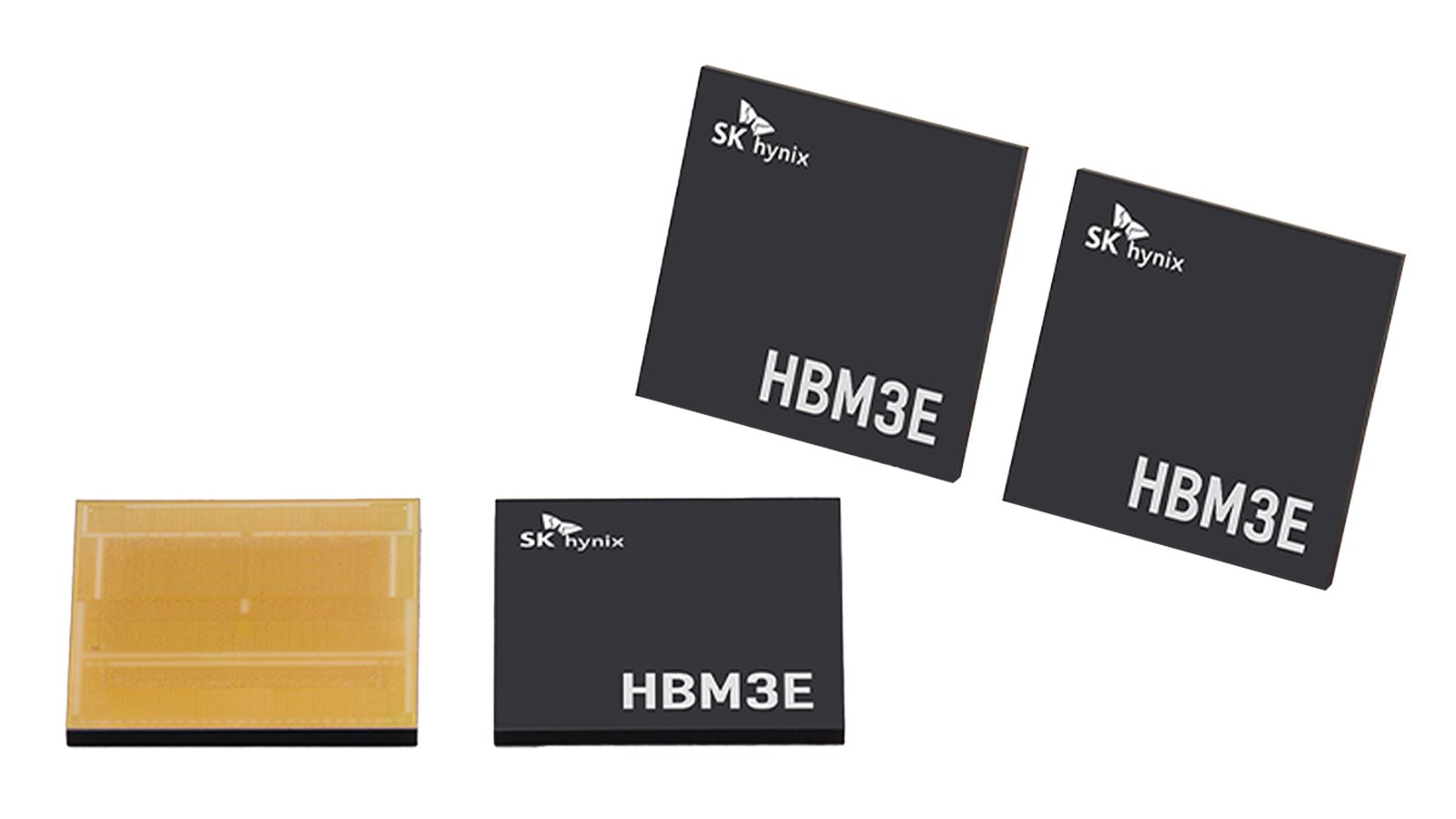
Wang Xiu, head of the SK Hynix GSM team, said: “Our company will start mass production next year and sales of HBM3E, which will further consolidate our leading position in the market."
He also said: "We plan to fully develop the follow-up product HBM4, so next year will represent SK hynix entering a new stage. This It will be a year worth celebrating for us."
He said that with the rapid development of the artificial intelligence industry, high-bandwidth memory (HBM) products will go beyond the current scope of artificial intelligence servers and expand to All fields related to artificial intelligence. He predicted that by then, our HBM products will play a very important role in leading the artificial intelligence industry
The query results show that SK Hynix has released three CXL-based solutions. SK Hynix said they will focus on promoting the commercialization of CXL next year and plan to develop and mass-produce a new generation of memory expansion solutions
Cui Yuanha, head of GSM, said: "We plan to complete 96GB in the first half of 2024 and customer certification of 128GB products, and will be commercialized in the second half of the year."
According to him, customers using the CXL 2.0 memory expansion solution can increase their bandwidth by 50% compared to systems that only carry DDR5 solutions. %, and the capacity can also be increased from 50% to 100%
The above is the detailed content of SK Hynix plans to accelerate the development of HBM4 and commercialize CXL memory to start mass production in 2024. For more information, please follow other related articles on the PHP Chinese website!

Hot AI Tools

Undresser.AI Undress
AI-powered app for creating realistic nude photos

AI Clothes Remover
Online AI tool for removing clothes from photos.

Undress AI Tool
Undress images for free

Clothoff.io
AI clothes remover

AI Hentai Generator
Generate AI Hentai for free.

Hot Article
Hot Tools

Notepad++7.3.1
Easy-to-use and free code editor

SublimeText3 Chinese version
Chinese version, very easy to use

Zend Studio 13.0.1
Powerful PHP integrated development environment

Dreamweaver CS6
Visual web development tools

SublimeText3 Mac version
God-level code editing software (SublimeText3)
Hot Topics
 1378
1378
 52
52

 Sources say SK Hynix's five-layer stacked 3D DRAM memory yield has reached 56.1%
Jun 24, 2024 pm 01:52 PM
Sources say SK Hynix's five-layer stacked 3D DRAM memory yield has reached 56.1%
Jun 24, 2024 pm 01:52 PM
According to news from this website on June 24, Korean media BusinessKorea reported that industry insiders revealed that SK Hynix published the latest research paper on 3D DRAM technology at the VLSI 2024 Summit held in Hawaii, USA from June 16 to 20. In this paper, SK Hynix reports that its five-layer stacked 3D DRAM memory yield has reached 56.1%, and the 3D DRAM in the experiment exhibits similar characteristics to current 2D DRAM. According to reports, unlike traditional DRAM, which arranges memory cells horizontally, 3D DRAM stacks cells vertically to achieve higher density in the same space. However, SK hynix
 Sources say Samsung Electronics and SK Hynix will commercialize stacked mobile memory after 2026
Sep 03, 2024 pm 02:15 PM
Sources say Samsung Electronics and SK Hynix will commercialize stacked mobile memory after 2026
Sep 03, 2024 pm 02:15 PM
According to news from this website on September 3, Korean media etnews reported yesterday (local time) that Samsung Electronics and SK Hynix’s “HBM-like” stacked structure mobile memory products will be commercialized after 2026. Sources said that the two Korean memory giants regard stacked mobile memory as an important source of future revenue and plan to expand "HBM-like memory" to smartphones, tablets and laptops to provide power for end-side AI. According to previous reports on this site, Samsung Electronics’ product is called LPWide I/O memory, and SK Hynix calls this technology VFO. The two companies have used roughly the same technical route, which is to combine fan-out packaging and vertical channels. Samsung Electronics’ LPWide I/O memory has a bit width of 512
 Hynix is the first to demonstrate UFS 4.1 flash memory: based on V9 TLC NAND particles
Aug 09, 2024 pm 03:33 PM
Hynix is the first to demonstrate UFS 4.1 flash memory: based on V9 TLC NAND particles
Aug 09, 2024 pm 03:33 PM
According to news on August 9, at the FMS2024 Summit, SK Hynix demonstrated its latest storage products, including UFS4.1 universal flash memory that has not yet officially released specifications. According to the official website of the JEDEC Solid State Technology Association, the latest UFS specification currently announced is UFS4.0 in August 2022. Its theoretical interface speed is as high as 46.4Gbps. It is expected that UFS4.1 will further improve the transmission rate. 1. Hynix demonstrated 512GB and 1TBUFS4.1 general-purpose flash memory products, based on 321-layer V91TbTLCNAND flash memory. SK Hynix also exhibited 3.2GbpsV92TbQLC and 3.6GbpsV9H1TbTLC particles. Hynix shows off V7-based
 SK Hynix takes the lead in demonstrating UFS 4.1 universal flash memory, based on V9 TLC NAND particles
Aug 09, 2024 am 10:42 AM
SK Hynix takes the lead in demonstrating UFS 4.1 universal flash memory, based on V9 TLC NAND particles
Aug 09, 2024 am 10:42 AM
According to news from this website on August 9, according to a press release issued by SK Hynix yesterday local time, the company demonstrated a series of new storage products at the FMS2024 Summit, including USF4.1 universal flash memory that has not yet officially released specifications. According to the official website of the JEDEC Solid State Technology Association, the latest UFS specification currently announced is UFS4.0 in August 2022. UFS4.0 specifies a theoretical interface speed of up to 46.4Gbps for each device, and USF4.1 is expected to further improve the transmission rate. ▲JEDECUFS specification page SK Hynix demonstrated two UFS4.1 general-purpose flash memories with capacities of 512GB and 1TB respectively, both based on the 321-layer stacked V91TbTLCNAND flash memory.
 It is reported that SK Hynix and Samsung Electronics have significantly expanded production of HBM memory this year, but the current yield rate is only 65%
Mar 05, 2024 pm 04:00 PM
It is reported that SK Hynix and Samsung Electronics have significantly expanded production of HBM memory this year, but the current yield rate is only 65%
Mar 05, 2024 pm 04:00 PM
According to news from this site on March 4, Korean media DealSite reported that SK Hynix and Samsung Electronics will significantly expand production of HBM memory this year. However, HBM memory has problems such as low yield, making it difficult to keep up with the demand related to the AI market. As a hot commodity in the AI semiconductor market, HBM memory uses wafer-level packaging (WLP): multi-layer DRAM memory wafers are connected to the basic wafer through TSV through silicon holes. A problem with one of the DRAM layers means that the entire HBM stack of scrapping. ▲HBM memory structure diagram. Image source: SK Hynix takes an 8-layer stacked product as an example. If the yield rate of each stack is 90%, then the yield rate of the overall HBM stack is only 43%, and more than half of the DRAM is discarded. And when HBM reaches the 12th floor,
 SK Hynix and Samsung Electronics are expected to start mass production of 1c nanometer DRAM memory within this year
Apr 09, 2024 pm 05:25 PM
SK Hynix and Samsung Electronics are expected to start mass production of 1c nanometer DRAM memory within this year
Apr 09, 2024 pm 05:25 PM
According to news from this site on April 9, Korean media Businesskorea reported that SK Hynix and Samsung Electronics are expected to start mass production of 1c nanometer DRAM memory within this year. After entering the 20~10nm process, memory generations are generally called in the form of 1+ letters. 1cnm corresponds to Micron's 1-gammanm expression and is the sixth 10+nm process generation. Samsung calls the previous generation 1bnm "12nm class". Samsung recently stated at the industry conference Memcon2024 that it plans to achieve mass production of 1cnm process by the end of this year; and recently, industry sources revealed that SK Hynix has internally formulated a roadmap for mass production of 1cnm DRAM memory in the third quarter. SK hynix plans to prepare in advance
 SK Hynix: CAMM memory is about to enter the desktop computer market
Jan 16, 2024 am 08:00 AM
SK Hynix: CAMM memory is about to enter the desktop computer market
Jan 16, 2024 am 08:00 AM
According to news from this site on January 15, SK Hynix revealed that the new CAMM memory standard is planning to enter the desktop field. CAMM is a new memory standard that is smaller and more compact than traditional DRAM modules and supports larger capacities. The standard has evolved into its second generation, LPCAMM2, which is used in notebook computers and thin and light PCs. LP stands for low power consumption, and the existing modules are based on the LPDDR5 or LPDDR5X standard and provide transmission speeds of up to 9.6Gbps. At CES2024, blogger ITSublssub visited the SK Hynix booth. The company’s representatives confirmed that the CAMM standard will enter the desktop platform. The first desktop platform CAMM product is also under development, but no specific details have been disclosed yet. burst
 SK Hynix releases big news: 238-layer 4D NAND flash memory is mass-produced, and mobile phone tests show that the speed is increased by 50%
Jun 09, 2023 am 08:14 AM
SK Hynix releases big news: 238-layer 4D NAND flash memory is mass-produced, and mobile phone tests show that the speed is increased by 50%
Jun 09, 2023 am 08:14 AM
According to news on June 8, South Korean memory manufacturer SK Hynix announced today that they have begun mass production of 238-layer 4D NAND flash memory chips. It is reported that SK Hynix is conducting product verification with overseas smartphone manufacturers. SK Hynix said that they have successfully developed a client SSD (ClientSSD) solution for smartphones and personal computers (PCs) and started mass production in May. Whether in 176-layer or 238-layer products, SK hynix has ensured world-leading competitiveness in terms of cost, performance and quality. According to the editor’s understanding, the 238-layer NAND flash memory chip is currently one of the smallest chips in the world. Compared with the previous generation’s 176-layer chip, its production is
