
 Technology peripherals
It Industry
It can reduce the use of expensive EUV lithography. Merck of Germany says DSA self-assembly technology will be commercially available within ten years.
Technology peripherals
It Industry
It can reduce the use of expensive EUV lithography. Merck of Germany says DSA self-assembly technology will be commercially available within ten years.
It can reduce the use of expensive EUV lithography. Merck of Germany says DSA self-assembly technology will be commercially available within ten years.

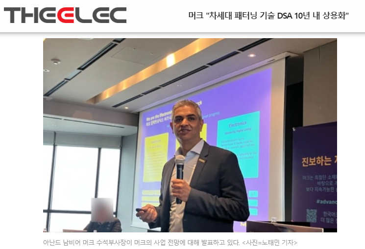
According to news from this website on February 5, Anand Nambier, senior vice president of Merck of Germany, said at a press conference recently that DSA self-assembly technology will be commercialized in the next ten years, can reduce expensive EUV patterning Times , becoming an important supplement to existing photolithography technology.
Note on this site: DSA stands for Directed self-assembly. It uses the surface characteristics of block copolymers to realize the automatic construction of periodic patterns. On this basis, it is induced to finally form the desired direction-controllable pattern. pattern. It is generally believed that DSA is not suitable for use as an independent patterning technology, but rather is combined with other patterning technologies (such as traditional photolithography) to produce high-precision semiconductors.
The main application of DSA in EUV is to compensate for the random error of EUV. Random errors account for 50% of the overall patterning error in EUV processes.
Commercial large-scale application of DSA also needs to solve some problems, such as reducing defects such as bubbles, bridges and clusters that occur during pattern generation. Among them, bridge defects are one of the most common problems.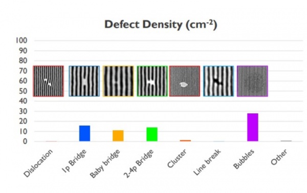 ▲ The occurrence of DSA technical defects. Image source imec
The above is the detailed content of It can reduce the use of expensive EUV lithography. Merck of Germany says DSA self-assembly technology will be commercially available within ten years.. For more information, please follow other related articles on the PHP Chinese website!

Hot AI Tools

Undresser.AI Undress
AI-powered app for creating realistic nude photos

AI Clothes Remover
Online AI tool for removing clothes from photos.

Undress AI Tool
Undress images for free

Clothoff.io
AI clothes remover

AI Hentai Generator
Generate AI Hentai for free.

Hot Article
Hot Tools

Notepad++7.3.1
Easy-to-use and free code editor

SublimeText3 Chinese version
Chinese version, very easy to use

Zend Studio 13.0.1
Powerful PHP integrated development environment

Dreamweaver CS6
Visual web development tools

SublimeText3 Mac version
God-level code editing software (SublimeText3)
Hot Topics
 1386
1386
 52
52

 1c nano generation memory competition: Samsung plans to increase the use of EUV, Micron will introduce molybdenum and ruthenium materials
Feb 04, 2024 am 09:40 AM
1c nano generation memory competition: Samsung plans to increase the use of EUV, Micron will introduce molybdenum and ruthenium materials
Feb 04, 2024 am 09:40 AM
Korean media TheElec reported that Samsung and Micron will introduce more new technologies in the next generation of DRAM memory, the 1cnm process. This move is expected to further improve memory performance and energy efficiency. As the main leaders in the global DRAM market, Samsung and Micron's technological innovation will promote the development of the entire industry. This also means that future memory products will be more efficient and powerful. Note from this site: The 1cnm generation is the sixth 10+nm generation, and Micron also calls it the 1γnm process. The most advanced memory currently is the 1bnm generation, and Samsung calls 1bnm a 12nm-level process. ChoiJeong-dong, senior vice president of analyst firm TechInsights, said at a recent seminar that Micron will be at the 1cnm Festival
 NVIDIA is not the only beneficiary, AI training also benefits memory chip manufacturers
May 31, 2023 pm 05:16 PM
NVIDIA is not the only beneficiary, AI training also benefits memory chip manufacturers
May 31, 2023 pm 05:16 PM
According to news on May 30, although the memory chip market is sluggish, there is a huge demand for artificial intelligence, which will benefit companies such as Samsung and SK Hynix. On May 24, Nvidia released its financial report, and the company’s market value surged by US$207 billion in two days. Previously, the semiconductor industry had been in a downturn, and this financial report forecast gave people great confidence and hope. If the field of artificial intelligence takes off, traditional technology giants like Microsoft and start-ups such as OpenAI will seek help from companies such as Samsung and SK Hynix. Machine learning requires memory chips to process large amounts of data, analyze video, audio and text, and simulate human creativity. In fact, AI companies may be buying more DRAM chips than ever before. Memory chip demand
 Is the 1nm chip made in China or the United States?
Nov 06, 2023 pm 01:30 PM
Is the 1nm chip made in China or the United States?
Nov 06, 2023 pm 01:30 PM
It is not certain who made the 1nm chip. From a research and development perspective, the 1nm chip was jointly developed by Taiwan, China and the United States. From a mass production perspective, this technology is not yet fully realized. The main person in charge of this research is Dr. Zhu Jiadi of MIT, who is a Chinese scientist. Dr. Zhu Jiadi said that the research is still in its early stages and is still a long way from mass production.
 First in China: Changxin Memory launches LPDDR5 DRAM memory chip
Nov 28, 2023 pm 09:29 PM
First in China: Changxin Memory launches LPDDR5 DRAM memory chip
Nov 28, 2023 pm 09:29 PM
News from this site on November 28. According to the official website of Changxin Memory, Changxin Memory has launched the latest LPDDR5DRAM memory chip. It is the first domestic brand to launch independently developed and produced LPDDR5 products, achieving a breakthrough in the domestic market and also making Changxin Storage's product layout in the mobile terminal market is more diversified. This website noticed that Changxin Memory LPDDR5 series products include 12Gb LPDDR5 particles, POP packaged 12GBLPDDR5 chips and DSC packaged 6GBLPDDR5 chips. The 12GBLPDDR5 chip has been verified on models of mainstream domestic mobile phone manufacturers such as Xiaomi and Transsion. LPDDR5 is a product launched by Changxin Storage for the mid-to-high-end mobile device market.
 Samsung is revealed to start installing its first ASML High-NA EUV lithography machine by the end of 2024 at the earliest
Aug 16, 2024 am 11:11 AM
Samsung is revealed to start installing its first ASML High-NA EUV lithography machine by the end of 2024 at the earliest
Aug 16, 2024 am 11:11 AM
According to news from this site on August 16, the Seoul Economic Daily reported yesterday (August 15) that Samsung will install its first High-NAEUV lithography machine from ASML between the fourth quarter of 2024 and the first quarter of 2025. It is expected to be put into use in mid-2025. Reports indicate that Samsung will install the first ASMLTwinscanEXE:5000High-NA lithography machine in its Hwaseong campus, which will be mainly used for research and development purposes to develop next-generation manufacturing technologies for logic and DRAM. Samsung plans to develop a strong ecosystem around High-NAEUV technology: In addition to acquiring high-NAEUV lithography equipment, Samsung is also cooperating with Japan's Lasertec to develop high-NAEUV lithography equipment specifically for High-NAEUV lithography equipment.
 It is reported that TSMC's advanced packaging customers are chasing orders significantly, and monthly production capacity is planned to increase by 120% next year
Nov 13, 2023 pm 12:29 PM
It is reported that TSMC's advanced packaging customers are chasing orders significantly, and monthly production capacity is planned to increase by 120% next year
Nov 13, 2023 pm 12:29 PM
News from this site on November 13, according to Taiwan Economic Daily, TSMC’s CoWoS advanced packaging demand is about to explode. In addition to NVIDIA, which has confirmed expanded orders in October, heavyweight customers such as Apple, AMD, Broadcom, and Marvell have also recently pursued orders significantly. According to reports, TSMC is working hard to accelerate the expansion of CoWoS advanced packaging production capacity to meet the needs of the above-mentioned five major customers. Next year's monthly production capacity is expected to increase by about 20% from the original target to 35,000 pieces. Analysts said that TSMC's five major customers have placed large orders, which shows that artificial intelligence applications have become widely popular, and major manufacturers are interested in artificial intelligence chips. The demand has increased significantly. Inquiries on this site found that the current CoWoS advanced packaging technology is mainly divided into three types - CoWos-S
 It is reported that Realtek 5GbE wired network card chip RTL8126-CG has stability issues and will be postponed to next year
Aug 25, 2023 am 11:53 AM
It is reported that Realtek 5GbE wired network card chip RTL8126-CG has stability issues and will be postponed to next year
Aug 25, 2023 am 11:53 AM
According to news from this site on August 24, most technology manufacturers displayed some new or upcoming new products at Gamescom. For example, ASRock showed its "half-generation" updated version of the Z790 motherboard. These new motherboards use The RTL8125-BG chip is used instead of the RTL8126-CG used in the prototype at the Computex show in June. According to Dutch media Tweakers, a number of motherboard manufacturers participating in Gamescom revealed that although Realtek's 5GbE wired network card chip RTL8126-CG is cheaper, it will not be installed on motherboards launched this fall due to stability issues. Realtek is said to be fixing this type of issue, but they won't be able to fix it before the new motherboards come out this fall
 Sources say NVIDIA is developing China-specific versions of AI chips HGX H20, L20 PCle and L2 PCle
Nov 09, 2023 pm 03:33 PM
Sources say NVIDIA is developing China-specific versions of AI chips HGX H20, L20 PCle and L2 PCle
Nov 09, 2023 pm 03:33 PM
The latest news shows that according to reports from the Science and Technology Innovation Board Daily and Blue Whale Finance, industry chain sources revealed that NVIDIA has developed the latest version of AI chips suitable for the Chinese market, including HGXH20, L20PCle and L2PCle. As of now, NVIDIA has not commented. People familiar with the matter said that these three chips are all based on improvements from NVIDIA H100. NVIDIA is expected to announce them as soon as November 16, and domestic manufacturers will get samples as soon as these days. After checking public information, we learned that NVIDIAH100TensorCoreGPU adopts the new Hopper architecture, which is based on TSMC N4 process and integrates 80 billion transistors. Compared with the previous generation product, it can provide multi-expert (MoE)
