
 Technology peripherals
It Industry
It is reported that Kioxia and SK Hynix are negotiating to produce HBM memory in Japan, which is expected to be a key step in the revival of Japanese semiconductors.
Technology peripherals
It Industry
It is reported that Kioxia and SK Hynix are negotiating to produce HBM memory in Japan, which is expected to be a key step in the revival of Japanese semiconductors.
It is reported that Kioxia and SK Hynix are negotiating to produce HBM memory in Japan, which is expected to be a key step in the revival of Japanese semiconductors.

According to news from this site on March 5, according to Japanese media Jiji News Agency, Kioxia and SK Hynix are in talks to produce HBM memory in Japan.
This site noticed that similar news came out last month, but the cooperation mentioned at that time was non-volatile memory, that is, NAND flash memory.

Currently, HBM memory, as one of the hot spots in the field of AI semiconductors, is increasingly in short supply. Taking SK Hynix as an example, they plan to increase production from 35,000 pieces per month in the second quarter of 2023 to 120,000-140,000 pieces by the end of the year. However, even so, this year's HBM quota has already been sold out. Expanding production capacity in Japan will help SK hynix meet market demand, thereby easing the current tight supply and demand situation.
According to reports, the two parties plan to use Kioxia’s existing factories in Kitakami and Yokkaichi, Japan, to quickly achieve production of HBM memory in Japan.
Currently, the storage semiconductor business of Kioxia and its partner Western Digital in Japan is limited to the NAND flash memory category.
HoweverIn the last century, Japanese manufacturers once dominated the DRAM memory market, but due to insufficient price competitiveness, they gradually gave way to South Korea and the United States. Manufacturers from both countries. With Elpida being acquired by Micron in 2012, Japanese manufacturers completely exited the memory market.
"Jiji News Agency" believes that, if the HBM memory cooperation between Kioxia and SK Hynix comes true, Japan will restart the production of advanced DRAM memory, becoming an important step in the revival of Japan's semiconductor industry .
SK Hynix indirectly holds some shares of Kioxia through Bain Capital, the largest shareholder of Kioxia. The opposition of SK Hynix is considered to be the decisive factor in the breakdown of merger negotiations between Kioxia and Western Digital last year.
Sources said that although obtaining the consent of SK Hynix is the key to promoting the next round of merger negotiations between Kioxia and Western Digital, but the cooperation on HBM memory is an independent negotiation content .
The above is the detailed content of It is reported that Kioxia and SK Hynix are negotiating to produce HBM memory in Japan, which is expected to be a key step in the revival of Japanese semiconductors.. For more information, please follow other related articles on the PHP Chinese website!

Hot AI Tools

Undresser.AI Undress
AI-powered app for creating realistic nude photos

AI Clothes Remover
Online AI tool for removing clothes from photos.

Undress AI Tool
Undress images for free

Clothoff.io
AI clothes remover

Video Face Swap
Swap faces in any video effortlessly with our completely free AI face swap tool!

Hot Article
Hot Tools

Notepad++7.3.1
Easy-to-use and free code editor

SublimeText3 Chinese version
Chinese version, very easy to use

Zend Studio 13.0.1
Powerful PHP integrated development environment

Dreamweaver CS6
Visual web development tools

SublimeText3 Mac version
God-level code editing software (SublimeText3)
Hot Topics
 1386
1386
 52
52

 Sources say SK Hynix's five-layer stacked 3D DRAM memory yield has reached 56.1%
Jun 24, 2024 pm 01:52 PM
Sources say SK Hynix's five-layer stacked 3D DRAM memory yield has reached 56.1%
Jun 24, 2024 pm 01:52 PM
According to news from this website on June 24, Korean media BusinessKorea reported that industry insiders revealed that SK Hynix published the latest research paper on 3D DRAM technology at the VLSI 2024 Summit held in Hawaii, USA from June 16 to 20. In this paper, SK Hynix reports that its five-layer stacked 3D DRAM memory yield has reached 56.1%, and the 3D DRAM in the experiment exhibits similar characteristics to current 2D DRAM. According to reports, unlike traditional DRAM, which arranges memory cells horizontally, 3D DRAM stacks cells vertically to achieve higher density in the same space. However, SK hynix
 Sources say Samsung Electronics and SK Hynix will commercialize stacked mobile memory after 2026
Sep 03, 2024 pm 02:15 PM
Sources say Samsung Electronics and SK Hynix will commercialize stacked mobile memory after 2026
Sep 03, 2024 pm 02:15 PM
According to news from this website on September 3, Korean media etnews reported yesterday (local time) that Samsung Electronics and SK Hynix’s “HBM-like” stacked structure mobile memory products will be commercialized after 2026. Sources said that the two Korean memory giants regard stacked mobile memory as an important source of future revenue and plan to expand "HBM-like memory" to smartphones, tablets and laptops to provide power for end-side AI. According to previous reports on this site, Samsung Electronics’ product is called LPWide I/O memory, and SK Hynix calls this technology VFO. The two companies have used roughly the same technical route, which is to combine fan-out packaging and vertical channels. Samsung Electronics’ LPWide I/O memory has a bit width of 512
 Micron: HBM memory consumes 3 times the wafer volume, and production capacity is basically booked for next year
Mar 22, 2024 pm 08:16 PM
Micron: HBM memory consumes 3 times the wafer volume, and production capacity is basically booked for next year
Mar 22, 2024 pm 08:16 PM
This site reported on March 21 that Micron held a conference call after releasing its quarterly financial report. At the conference, Micron CEO Sanjay Mehrotra said that compared to traditional memory, HBM consumes significantly more wafers. Micron said that when producing the same capacity at the same node, the current most advanced HBM3E memory consumes three times more wafers than standard DDR5, and it is expected that as performance improves and packaging complexity intensifies, in the future HBM4 This ratio will further increase. Referring to previous reports on this site, this high ratio is partly due to HBM’s low yield rate. HBM memory is stacked with multi-layer DRAM memory TSV connections. A problem with one layer means that the entire
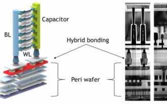
 Samsung announced the completion of 16-layer hybrid bonding stacking process technology verification, which is expected to be widely used in HBM4 memory
Apr 07, 2024 pm 09:19 PM
Samsung announced the completion of 16-layer hybrid bonding stacking process technology verification, which is expected to be widely used in HBM4 memory
Apr 07, 2024 pm 09:19 PM
According to the report, Samsung Electronics executive Dae Woo Kim said that at the 2024 Korean Microelectronics and Packaging Society Annual Meeting, Samsung Electronics will complete the verification of the 16-layer hybrid bonding HBM memory technology. It is reported that this technology has passed technical verification. The report also stated that this technical verification will lay the foundation for the development of the memory market in the next few years. DaeWooKim said that Samsung Electronics has successfully manufactured a 16-layer stacked HBM3 memory based on hybrid bonding technology. The memory sample works normally. In the future, the 16-layer stacked hybrid bonding technology will be used for mass production of HBM4 memory. ▲Image source TheElec, same as below. Compared with the existing bonding process, hybrid bonding does not need to add bumps between DRAM memory layers, but directly connects the upper and lower layers copper to copper.
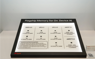 Hynix is the first to demonstrate UFS 4.1 flash memory: based on V9 TLC NAND particles
Aug 09, 2024 pm 03:33 PM
Hynix is the first to demonstrate UFS 4.1 flash memory: based on V9 TLC NAND particles
Aug 09, 2024 pm 03:33 PM
According to news on August 9, at the FMS2024 Summit, SK Hynix demonstrated its latest storage products, including UFS4.1 universal flash memory that has not yet officially released specifications. According to the official website of the JEDEC Solid State Technology Association, the latest UFS specification currently announced is UFS4.0 in August 2022. Its theoretical interface speed is as high as 46.4Gbps. It is expected that UFS4.1 will further improve the transmission rate. 1. Hynix demonstrated 512GB and 1TBUFS4.1 general-purpose flash memory products, based on 321-layer V91TbTLCNAND flash memory. SK Hynix also exhibited 3.2GbpsV92TbQLC and 3.6GbpsV9H1TbTLC particles. Hynix shows off V7-based
 SK Hynix takes the lead in demonstrating UFS 4.1 universal flash memory, based on V9 TLC NAND particles
Aug 09, 2024 am 10:42 AM
SK Hynix takes the lead in demonstrating UFS 4.1 universal flash memory, based on V9 TLC NAND particles
Aug 09, 2024 am 10:42 AM
According to news from this website on August 9, according to a press release issued by SK Hynix yesterday local time, the company demonstrated a series of new storage products at the FMS2024 Summit, including USF4.1 universal flash memory that has not yet officially released specifications. According to the official website of the JEDEC Solid State Technology Association, the latest UFS specification currently announced is UFS4.0 in August 2022. UFS4.0 specifies a theoretical interface speed of up to 46.4Gbps for each device, and USF4.1 is expected to further improve the transmission rate. ▲JEDECUFS specification page SK Hynix demonstrated two UFS4.1 general-purpose flash memories with capacities of 512GB and 1TB respectively, both based on the 321-layer stacked V91TbTLCNAND flash memory.
 It is reported that SK Hynix and Samsung Electronics have significantly expanded production of HBM memory this year, but the current yield rate is only 65%
Mar 05, 2024 pm 04:00 PM
It is reported that SK Hynix and Samsung Electronics have significantly expanded production of HBM memory this year, but the current yield rate is only 65%
Mar 05, 2024 pm 04:00 PM
According to news from this site on March 4, Korean media DealSite reported that SK Hynix and Samsung Electronics will significantly expand production of HBM memory this year. However, HBM memory has problems such as low yield, making it difficult to keep up with the demand related to the AI market. As a hot commodity in the AI semiconductor market, HBM memory uses wafer-level packaging (WLP): multi-layer DRAM memory wafers are connected to the basic wafer through TSV through silicon holes. A problem with one of the DRAM layers means that the entire HBM stack of scrapping. ▲HBM memory structure diagram. Image source: SK Hynix takes an 8-layer stacked product as an example. If the yield rate of each stack is 90%, then the yield rate of the overall HBM stack is only 43%, and more than half of the DRAM is discarded. And when HBM reaches the 12th floor,
 Born for AI: Samsung says it will put HBM4 video memory into production in 2025, competing for leadership in high-performance computing
Oct 13, 2023 pm 02:17 PM
Born for AI: Samsung says it will put HBM4 video memory into production in 2025, competing for leadership in high-performance computing
Oct 13, 2023 pm 02:17 PM
The rapid increase in AI computing power in recent years has made computing cards a new sought-after target for major hardware manufacturers. In particular, computing cards launched by companies like NVIDIA are in short supply. In addition to NVIDIA launching powerful GPUs, including Samsung Storage manufacturers such as Hynix and Hynix do not want to miss this AI feast, especially high-performance computing cards that require high-performance graphics memory produced by them. Currently, a senior executive in the storage field of Samsung issued a document saying that Samsung plans to mass-produce the latest memory in 2025. HBM4 video memory, thus surpassing Hynix. In 2016, Samsung officially began mass production of HBM video memory. Compared with GDDR video memory, HBM video memory has larger bandwidth, thereby achieving higher performance transmission. In the consumer market, AMD’s Radeon
