
 Hardware Tutorial
Hardware News
SK Hynix demonstrates 40Gbps ultra-high-speed GDDR7 video memory
Hardware Tutorial
Hardware News
SK Hynix demonstrates 40Gbps ultra-high-speed GDDR7 video memory
SK Hynix demonstrates 40Gbps ultra-high-speed GDDR7 video memory

According to news from this site on March 21, Samsung demonstrated its upcoming 28Gbps and 32Gbps GDDR7 video memory at the GTC 2024 exhibition, and Hynix went one step further. The company is developing faster video memory modules.
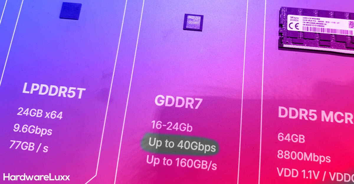
According to HardwareLuxx, Samsung previously claimed to be developing 37Gbps GDDR7 video memory, which is currently the fastest known such memory. Hynix has set its target at a higher 40Gbps, which may become the performance target for its entire G7 series of graphics memories.
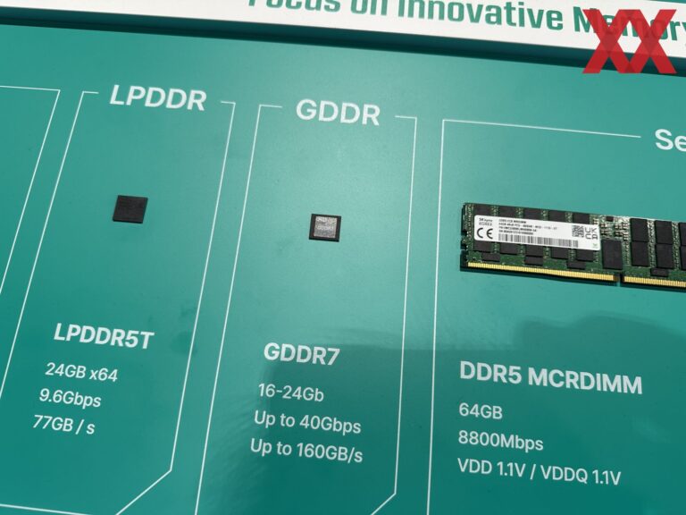
This site noticed that the new generation of GDDR7 memory will also provide higher capacity options. The versions displayed this time include 16Gb and 24Gb styles (corresponding to 2GB and 3GB respectively) memory capacity). According to the specifications announced by the JEDEC organization, the speed of GDDR7 memory is expected to be further increased to 48Gbps in the future, and the capacity will also reach 64Gb (8GB), which will bring a huge leap in video memory capacity. A standard 256-bit graphics card interface paired with such memory will provide up to 64GB of graphics memory, which is a huge improvement compared to the current maximum of 16GB.
In addition, SK Hynix also demonstrated DDR5 MCR DIMM memory modules with a transfer rate of up to 8800 MT/s, a capacity of up to 64GB, and a voltage of 1.1V.
Currently, the NVIDIA RTX 50 series graphics cards, which are expected to be launched by the end of the year, will be the first products to use GDDR7 video memory. According to reports, this series of graphics cards will use 28Gbps memory speed, leaving room for speed increases of more than 32Gbps for next-generation products.
The above is the detailed content of SK Hynix demonstrates 40Gbps ultra-high-speed GDDR7 video memory. For more information, please follow other related articles on the PHP Chinese website!

Hot AI Tools

Undresser.AI Undress
AI-powered app for creating realistic nude photos

AI Clothes Remover
Online AI tool for removing clothes from photos.

Undress AI Tool
Undress images for free

Clothoff.io
AI clothes remover

AI Hentai Generator
Generate AI Hentai for free.

Hot Article
Hot Tools

Notepad++7.3.1
Easy-to-use and free code editor

SublimeText3 Chinese version
Chinese version, very easy to use

Zend Studio 13.0.1
Powerful PHP integrated development environment

Dreamweaver CS6
Visual web development tools

SublimeText3 Mac version
God-level code editing software (SublimeText3)
Hot Topics
 1371
1371
 52
52

 How to increase VRAM in Windows 11
May 05, 2023 pm 04:25 PM
How to increase VRAM in Windows 11
May 05, 2023 pm 04:25 PM
Are you receiving warnings about your computer's graphics card memory when using graphics-intensive software or a new game? To prevent these issues and run resource-intensive games or applications smoothly, you need a graphics card and RAM that meet its specifications. Whether your computer is old or has graphics issues for no apparent reason, you can fix the problem by adjusting a few parameters in certain situations. The method we will cover in this article is to increase VRAM in Windows 11, which is one of the most effective ways to get the most out of your computer, especially your graphics card. But before we get into it, let's see what VRAM is and what it does. So, without further ado, let’s get started. Why increase video memory? What aspects of gaming and graphics software do we need to point out?
 Sources say SK Hynix's five-layer stacked 3D DRAM memory yield has reached 56.1%
Jun 24, 2024 pm 01:52 PM
Sources say SK Hynix's five-layer stacked 3D DRAM memory yield has reached 56.1%
Jun 24, 2024 pm 01:52 PM
According to news from this website on June 24, Korean media BusinessKorea reported that industry insiders revealed that SK Hynix published the latest research paper on 3D DRAM technology at the VLSI 2024 Summit held in Hawaii, USA from June 16 to 20. In this paper, SK Hynix reports that its five-layer stacked 3D DRAM memory yield has reached 56.1%, and the 3D DRAM in the experiment exhibits similar characteristics to current 2D DRAM. According to reports, unlike traditional DRAM, which arranges memory cells horizontally, 3D DRAM stacks cells vertically to achieve higher density in the same space. However, SK hynix
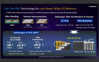 Sources say Samsung Electronics and SK Hynix will commercialize stacked mobile memory after 2026
Sep 03, 2024 pm 02:15 PM
Sources say Samsung Electronics and SK Hynix will commercialize stacked mobile memory after 2026
Sep 03, 2024 pm 02:15 PM
According to news from this website on September 3, Korean media etnews reported yesterday (local time) that Samsung Electronics and SK Hynix’s “HBM-like” stacked structure mobile memory products will be commercialized after 2026. Sources said that the two Korean memory giants regard stacked mobile memory as an important source of future revenue and plan to expand "HBM-like memory" to smartphones, tablets and laptops to provide power for end-side AI. According to previous reports on this site, Samsung Electronics’ product is called LPWide I/O memory, and SK Hynix calls this technology VFO. The two companies have used roughly the same technical route, which is to combine fan-out packaging and vertical channels. Samsung Electronics’ LPWide I/O memory has a bit width of 512
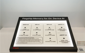 Hynix is the first to demonstrate UFS 4.1 flash memory: based on V9 TLC NAND particles
Aug 09, 2024 pm 03:33 PM
Hynix is the first to demonstrate UFS 4.1 flash memory: based on V9 TLC NAND particles
Aug 09, 2024 pm 03:33 PM
According to news on August 9, at the FMS2024 Summit, SK Hynix demonstrated its latest storage products, including UFS4.1 universal flash memory that has not yet officially released specifications. According to the official website of the JEDEC Solid State Technology Association, the latest UFS specification currently announced is UFS4.0 in August 2022. Its theoretical interface speed is as high as 46.4Gbps. It is expected that UFS4.1 will further improve the transmission rate. 1. Hynix demonstrated 512GB and 1TBUFS4.1 general-purpose flash memory products, based on 321-layer V91TbTLCNAND flash memory. SK Hynix also exhibited 3.2GbpsV92TbQLC and 3.6GbpsV9H1TbTLC particles. Hynix shows off V7-based
 SK Hynix takes the lead in demonstrating UFS 4.1 universal flash memory, based on V9 TLC NAND particles
Aug 09, 2024 am 10:42 AM
SK Hynix takes the lead in demonstrating UFS 4.1 universal flash memory, based on V9 TLC NAND particles
Aug 09, 2024 am 10:42 AM
According to news from this website on August 9, according to a press release issued by SK Hynix yesterday local time, the company demonstrated a series of new storage products at the FMS2024 Summit, including USF4.1 universal flash memory that has not yet officially released specifications. According to the official website of the JEDEC Solid State Technology Association, the latest UFS specification currently announced is UFS4.0 in August 2022. UFS4.0 specifies a theoretical interface speed of up to 46.4Gbps for each device, and USF4.1 is expected to further improve the transmission rate. ▲JEDECUFS specification page SK Hynix demonstrated two UFS4.1 general-purpose flash memories with capacities of 512GB and 1TB respectively, both based on the 321-layer stacked V91TbTLCNAND flash memory.
 It is reported that SK Hynix and Samsung Electronics have significantly expanded production of HBM memory this year, but the current yield rate is only 65%
Mar 05, 2024 pm 04:00 PM
It is reported that SK Hynix and Samsung Electronics have significantly expanded production of HBM memory this year, but the current yield rate is only 65%
Mar 05, 2024 pm 04:00 PM
According to news from this site on March 4, Korean media DealSite reported that SK Hynix and Samsung Electronics will significantly expand production of HBM memory this year. However, HBM memory has problems such as low yield, making it difficult to keep up with the demand related to the AI market. As a hot commodity in the AI semiconductor market, HBM memory uses wafer-level packaging (WLP): multi-layer DRAM memory wafers are connected to the basic wafer through TSV through silicon holes. A problem with one of the DRAM layers means that the entire HBM stack of scrapping. ▲HBM memory structure diagram. Image source: SK Hynix takes an 8-layer stacked product as an example. If the yield rate of each stack is 90%, then the yield rate of the overall HBM stack is only 43%, and more than half of the DRAM is discarded. And when HBM reaches the 12th floor,
 New AI algorithm unveiled: power reduced to 1/50 of conventional configuration, memory usage reduced to 1/10
Jun 27, 2024 pm 03:54 PM
New AI algorithm unveiled: power reduced to 1/50 of conventional configuration, memory usage reduced to 1/10
Jun 27, 2024 pm 03:54 PM
According to news from this site on June 27, a research team from the University of California, Santa Cruz has developed a new method that can run a large language model with a scale of 1 billion parameters using only 13W of power (equivalent to the power of a modern LED light bulb). . For comparison, a data center-level GPU used for large language model tasks requires about 700W. Under the AI wave, the main research directions of many companies and institutions are application and reasoning, and indicators such as efficiency are rarely considered. To alleviate this situation, the researcher eliminated the intensive technique of matrix multiplication and proposed a "ternion" solution, which has only three values of negative one, zero, or positive one. The team also created custom hardware using a highly customized circuit called a field-programmable gate array (FPGA), allowing them to maximize the use of
 SK Hynix and Samsung Electronics are expected to start mass production of 1c nanometer DRAM memory within this year
Apr 09, 2024 pm 05:25 PM
SK Hynix and Samsung Electronics are expected to start mass production of 1c nanometer DRAM memory within this year
Apr 09, 2024 pm 05:25 PM
According to news from this site on April 9, Korean media Businesskorea reported that SK Hynix and Samsung Electronics are expected to start mass production of 1c nanometer DRAM memory within this year. After entering the 20~10nm process, memory generations are generally called in the form of 1+ letters. 1cnm corresponds to Micron's 1-gammanm expression and is the sixth 10+nm process generation. Samsung calls the previous generation 1bnm "12nm class". Samsung recently stated at the industry conference Memcon2024 that it plans to achieve mass production of 1cnm process by the end of this year; and recently, industry sources revealed that SK Hynix has internally formulated a roadmap for mass production of 1cnm DRAM memory in the third quarter. SK hynix plans to prepare in advance
