 Technology peripherals
 It Industry
 Our country's scientific research team completed preliminary verification of new photoresist technology, which has better performance than most commercial photoresists
Our country's scientific research team completed preliminary verification of new photoresist technology, which has better performance than most commercial photoresists
According to Hubei Jiufengshan Laboratory, as an indispensable material for semiconductor manufacturing, photoresist quality and performance are key factors affecting the electrical performance, yield and reliability of integrated circuit circuits. However, the technical threshold for photoresist is high, and there are only a handful of photoresist products on the market that have high process stability, wide process tolerance, and strong universal applicability. When semiconductor manufacturing chips reach 100 nm or even below 10 nm, how to produce photolithography patterns with high resolution, excellent cross-sectional morphology, and low line edge defects has become a common problem in photolithography manufacturing.
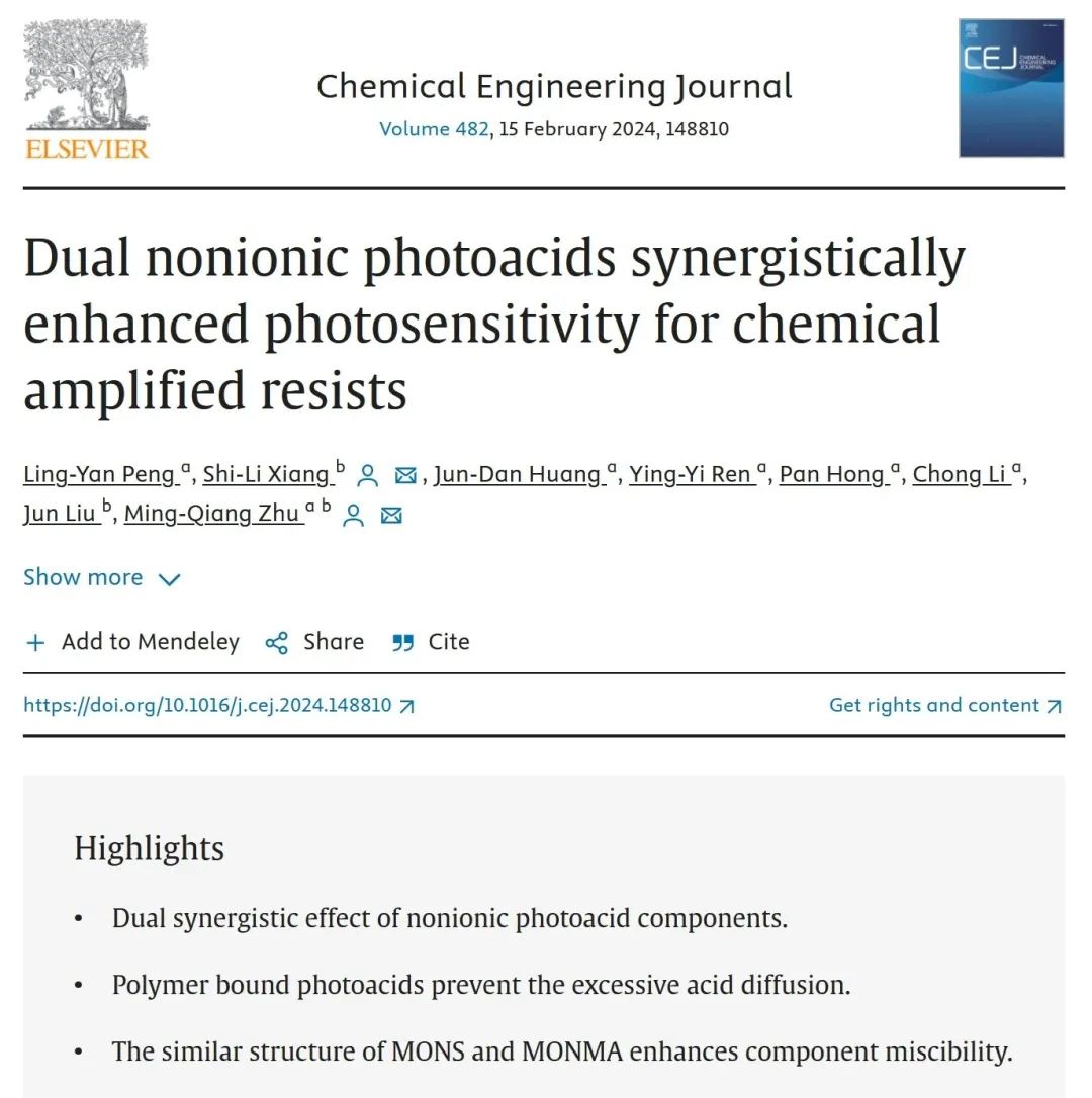
In response to the above bottleneck problem, Jiufengshan Laboratory and Huazhong University of Science and Technology formed a joint research team, supported the Huazhong University of Science and Technology team to break through the "chemical amplification photoresist with dual non-ionic photoacid synergistically enhanced response" technology.
Through ingenious chemical structure design, this research uses two photosensitive units to construct a "chemical amplification photoresist with dual non-ionic photoacid synergistically enhanced response", and finally obtains the lithography image morphology and line edge roughness Excellent accuracy, the standard deviation (SD) of the normal distribution of space pattern width values is extremely small (about 0.05), and performance is better than most commercial photoresists. Moreover, the time required for each step of photolithography and development fully meets the requirements for throughput and production efficiency in semiconductor mass production manufacturing.
The research results are expected to provide clear directions for common problems in photolithography manufacturing, and at the same time provide technical reserves for the development of EUV photoresist.

The relevant results, titled "Dual nonionic photoacids synergistically enhanced photosensitivity for chemical amplified resists", were published in top international publications on February 15, 2024 Published in Chemical Engineering Journal (IF=15.1).
This project is co-funded by the China Natural Science Foundation (1973 Program, mainly as Professor Zhu Mingqiang of the Optoelectronics National Research Center of Huazhong University of Science and Technology, Professor Shi Jun and Dr. Xiang Shili of the Hubei Jiufengshan Laboratory Technology Center.)
Relying on the Jiufengshan laboratory process platform, the above-mentioned photoresist system with independent intellectual property rights has completed preliminary process verification on the production line, and simultaneously completed the detection and optimization of various technical indicators , realizing the entire chain from technology development to achievement transformation.
Attached to the paper link on this site:
https://doi.org/10.1016/j.cej.2024.148810
The above is the detailed content of Our country's scientific research team completed preliminary verification of new photoresist technology, which has better performance than most commercial photoresists. For more information, please follow other related articles on the PHP Chinese website!

Hot AI Tools

Undresser.AI Undress
AI-powered app for creating realistic nude photos

AI Clothes Remover
Online AI tool for removing clothes from photos.

Undress AI Tool
Undress images for free

Clothoff.io
AI clothes remover

AI Hentai Generator
Generate AI Hentai for free.

Hot Article

Hot Tools

Notepad++7.3.1
Easy-to-use and free code editor

SublimeText3 Chinese version
Chinese version, very easy to use

Zend Studio 13.0.1
Powerful PHP integrated development environment

Dreamweaver CS6
Visual web development tools

SublimeText3 Mac version
God-level code editing software (SublimeText3)

Hot Topics
 Innolux plans to mass-produce fan-out panel-level semiconductor packaging technology by the end of the year
Aug 07, 2024 pm 06:18 PM
According to news from this site on August 6, Yang Zhuxiang, general manager of Innolux Corporation, said yesterday (August 5) that the company is actively deploying and promoting semiconductor fan-out panel-level packaging (FOPLP) and is expected to mass-produce ChipFirst before the end of this year. The contribution of process technology to revenue will be apparent in the first quarter of next year. Fenye Innolux stated that it is expected to mass-produce the redistribution layer (RDLFirst) process technology for mid-to-high-end products in the next 1-2 years, and will work with partners to develop the most technically difficult glass drilling (TGV) process, which will take another 2-3 years. It can be put into mass production within a year. Yang Zhuxiang said that Innolux’s FOPLP technology is “ready for mass production” and will enter the market with low-end and mid-range products.
 Is the 1nm chip made in China or the United States?
Nov 06, 2023 pm 01:30 PM
It is not certain who made the 1nm chip. From a research and development perspective, the 1nm chip was jointly developed by Taiwan, China and the United States. From a mass production perspective, this technology is not yet fully realized. The main person in charge of this research is Dr. Zhu Jiadi of MIT, who is a Chinese scientist. Dr. Zhu Jiadi said that the research is still in its early stages and is still a long way from mass production.
 First in China: Changxin Memory launches LPDDR5 DRAM memory chip
Nov 28, 2023 pm 09:29 PM
News from this site on November 28. According to the official website of Changxin Memory, Changxin Memory has launched the latest LPDDR5DRAM memory chip. It is the first domestic brand to launch independently developed and produced LPDDR5 products, achieving a breakthrough in the domestic market and also making Changxin Storage's product layout in the mobile terminal market is more diversified. This website noticed that Changxin Memory LPDDR5 series products include 12Gb LPDDR5 particles, POP packaged 12GBLPDDR5 chips and DSC packaged 6GBLPDDR5 chips. The 12GBLPDDR5 chip has been verified on models of mainstream domestic mobile phone manufacturers such as Xiaomi and Transsion. LPDDR5 is a product launched by Changxin Storage for the mid-to-high-end mobile device market.
 It is reported that TSMC's advanced packaging customers are chasing orders significantly, and monthly production capacity is planned to increase by 120% next year
Nov 13, 2023 pm 12:29 PM
News from this site on November 13, according to Taiwan Economic Daily, TSMC’s CoWoS advanced packaging demand is about to explode. In addition to NVIDIA, which has confirmed expanded orders in October, heavyweight customers such as Apple, AMD, Broadcom, and Marvell have also recently pursued orders significantly. According to reports, TSMC is working hard to accelerate the expansion of CoWoS advanced packaging production capacity to meet the needs of the above-mentioned five major customers. Next year's monthly production capacity is expected to increase by about 20% from the original target to 35,000 pieces. Analysts said that TSMC's five major customers have placed large orders, which shows that artificial intelligence applications have become widely popular, and major manufacturers are interested in artificial intelligence chips. The demand has increased significantly. Inquiries on this site found that the current CoWoS advanced packaging technology is mainly divided into three types - CoWos-S
 TrendForce: Nvidia's Blackwell platform products drive TSMC's CoWoS production capacity to increase by 150% this year
Apr 17, 2024 pm 08:00 PM
According to news from this site on April 17, TrendForce recently released a report, believing that demand for Nvidia's new Blackwell platform products is bullish, and is expected to drive TSMC's total CoWoS packaging production capacity to increase by more than 150% in 2024. NVIDIA Blackwell's new platform products include B-series GPUs and GB200 accelerator cards integrating NVIDIA's own GraceArm CPU. TrendForce confirms that the supply chain is currently very optimistic about GB200. It is estimated that shipments in 2025 are expected to exceed one million units, accounting for 40-50% of Nvidia's high-end GPUs. Nvidia plans to deliver products such as GB200 and B100 in the second half of the year, but upstream wafer packaging must further adopt more complex products.
 SK hynix's innovative semiconductor CMP polishing pad technology enables sustainable use
Dec 28, 2023 pm 11:04 PM
According to news from this website on December 27, according to Korean media ETNews, SK Hynix has recently developed reusable CMP polishing pad technology, which can not only reduce costs, but also enhance ESG (environmental, social, governance) management. SK Hynix said that they will first deploy reusable CMP polishing pads in low-risk processes and gradually expand their application scope. Note: CMP technology is to make the surface of the material to be polished under the combined action of chemicals and mechanics. A process to achieve the required flatness. The chemical components in the polishing fluid react chemically with the material surface to form a softened layer that is easy to polish. The polishing pad and abrasive particles in the polishing fluid physically and mechanically polish the material surface to remove the softened layer. Source: Dinglong shares in CM
 Sony Group: Its semiconductor factories concealed emissions of harmful substances
Jul 12, 2024 pm 02:09 PM
According to reports from this website on July 8, based on reports from Nikkei and Japan's "Jiji News Agency", on the 8th (today) local time, Sony Semiconductor Manufacturing Company, a semiconductor manufacturer under the Sony Group, announced that the company had discharged harmful chemicals outside the factory. , and no notification was made. The company said this was due to an input error and an imperfect confirmation system. In fiscal years 2021 and 2022, the camera image sensor factory located in Kikuyo Town, Kumamoto Prefecture, incorrectly reported its emissions of chemical substances as 0. The actual situation was that there were emissions of "waste without harmless treatment." The plant emits hydrogen fluoride, which is commonly used in semiconductor processing and cleaning. Note from this site: Hydrogen fluoride is harmful to the human body and can cause respiratory diseases and even life-threatening effects when inhaled. sony half
 Samsung plans to invest 10 trillion won in semiconductor equipment and purchase ASML EUV lithography machines in large quantities
Nov 15, 2023 pm 12:33 PM
Samsung plans to increase the import of more ASML extreme ultraviolet (EUV) lithography equipment, according to a report from South Korea's Electronic News Today. Although the confidentiality clause in the contract did not disclose specific details, according to securities market news, this agreement will allow ASML to A total of 50 sets of equipment will be provided within five years. The unit price of each equipment is approximately 200 billion won (approximately 1.102 billion yuan), and the total value can reach 10 trillion won (approximately 55.1 billion yuan). It is currently unclear what the contract The product is an existing EUV lithography equipment or a next-generation "HighNAEUV" lithography equipment. However, the biggest problem with current EUV lithography equipment is limited output. According to officials, it is "more complex than satellite components" and can only be produced in very limited quantities each year. according to


