
 Technology peripherals
It Industry
Kioxia aims to launch 1,000-layer NAND flash memory in 2031 to reorganize storage-class memory business
Technology peripherals
It Industry
Kioxia aims to launch 1,000-layer NAND flash memory in 2031 to reorganize storage-class memory business
Kioxia aims to launch 1,000-layer NAND flash memory in 2031 to reorganize storage-class memory business


According to Nikkei xTECH, Kioxia CTO Hideshi Miyajima said at the recent 71st Spring Academic Lecture of the Japan Society of Applied Physics that the company aims to launch in 2030~2031 1000-layer 3D NAND flash memory and reorganized the storage class memory (SCM) business.
KIOXIA and Western Digital are working together to develop NAND flash memory technology. The most advanced product of the current partners is the 218-layer stacked BICS8 3D flash memory. BICS8 flash memory can achieve an I/O rate of 3200MT/s.
In 2022, another major NAND company demonstrated a similar view at Technology Day. It is predicted that by 2030, they plan to achieve 1,000-layer stacked 3D NAND storage.
Increasing the number of stacking layers is the main way to increase the capacity of a single 3D NAND flash memory particle. However, as the number of layers increases, the difficulty of etching vertical channels in flash memory particles gradually increases as the aspect ratio increases. In addition to high difficulty and low yield, high aspect ratio etching is also a time-consuming and costly process: currently each such etching takes about 1 hour. If NAND factories want to increase production capacity, they must purchase More etching machines.
Therefore
KioXia uses a dual-stack processin BICS8 to achieve vertical channel etching of the two NAND stacks separately. This move increases the trouble of passage between dual stacks, but overall it still reduces the difficulty. Thousand-layer stacked NAND flash memory is expected to contain more NAND stacks in the future.
In addition, Miyajima Hideshi also said that compared to competitors that operate both NAND and DRAM,
Kioxia is at a competitive disadvantage in terms of business richness, so it is necessary to cultivate storage-class memory (SCM), etc. New storage product business. The CTO said that under the AI boom, the performance gap between DRAM and NAND is widening, and SCM can fill this gap.
KioXia reorganized the previous "Memory Technology Research Laboratory" into the "Advanced Technology Research Laboratory" on April 1. Its SCM research will focus on new memories such as MRAM, FeRAM, and ReRAM, which are expected to be shipped within 2 to 3 years.
Referring to reports on this site, Kioxia previously focused on XL-FLASH flash memory solutions in the SCM field. The company launched the second generation of XL-FLASH in 2022 that supports MLC mode.
The above is the detailed content of Kioxia aims to launch 1,000-layer NAND flash memory in 2031 to reorganize storage-class memory business. For more information, please follow other related articles on the PHP Chinese website!

Hot AI Tools

Undresser.AI Undress
AI-powered app for creating realistic nude photos

AI Clothes Remover
Online AI tool for removing clothes from photos.

Undress AI Tool
Undress images for free

Clothoff.io
AI clothes remover

Video Face Swap
Swap faces in any video effortlessly with our completely free AI face swap tool!

Hot Article
Hot Tools

Notepad++7.3.1
Easy-to-use and free code editor

SublimeText3 Chinese version
Chinese version, very easy to use

Zend Studio 13.0.1
Powerful PHP integrated development environment

Dreamweaver CS6
Visual web development tools

SublimeText3 Mac version
God-level code editing software (SublimeText3)
Hot Topics
 1392
1392
 52
52

 Fix: Rufus error when formatting on Windows 11
Apr 28, 2023 pm 05:28 PM
Fix: Rufus error when formatting on Windows 11
Apr 28, 2023 pm 05:28 PM
Rufus is an excellent tool for creating bootable installation media, and many people use it to perform a clean installation of Windows on their PC. However, many users have reported Rufus errors on Windows 11. These errors will prevent you from creating installation media, thereby preventing you from installing Windows 11 or any other operating system. Fortunately, fixing these problems is relatively simple, and in today's tutorial, we'll show you the best methods you can use to fix this problem. Why do I get an undetermined error when formatting in Rufus on Windows 11? There are many reasons for this, and in most cases, it's just a software glitch that causes the problem. You can pass
 Commands to install BalenaEtcher on Windows 11
Apr 19, 2023 pm 05:46 PM
Commands to install BalenaEtcher on Windows 11
Apr 19, 2023 pm 05:46 PM
Steps to Install BalenaEtcher on Windows 11 Here we will show the quick way to install BalenaEthcer on Windows 11 without visiting its official website. 1. Open a command terminal (as an administrator), right-click the Start button and select Terminal (Admin). This will open a Windows Terminal with administrative rights to install software and perform other important tasks as superuser. 2. Install BalenaEtcher on Windows 11 Now, on your Windows terminal, just run Using the default Windows package manager
 Industry's highest transfer rate of 3.6GB/s, Micron announces mass production of ninth-generation 276-layer TLC NAND flash memory
Jul 31, 2024 am 08:05 AM
Industry's highest transfer rate of 3.6GB/s, Micron announces mass production of ninth-generation 276-layer TLC NAND flash memory
Jul 31, 2024 am 08:05 AM
According to news from this site on July 30, Micron announced today (local time) that its ninth generation (site note: 276 layers) 3DTLC NAND flash memory will be mass-produced and shipped. Micron said that its G9NAND has the industry's highest I/O transfer rate of 3.6GB/s (i.e. 3600MT/s flash memory interface rate), which is 50% higher than the existing competing products of 2400MT/s, and can better meet the needs of data-intensive workloads. High throughput requirements. At the same time, Micron's G9NAND is 99% and 88% higher than other solutions on the market in terms of write bandwidth and read bandwidth respectively. This NAND particle-level advantage will bring performance and energy efficiency to solid-state drives and embedded storage solutions. improvement. In addition, like previous generations of Micron NAND flash memory, Micron 276
 Samsung's 9th generation V-NAND metal wiring mass production process is revealed to use molybdenum technology for the first time
Jul 03, 2024 pm 05:39 PM
Samsung's 9th generation V-NAND metal wiring mass production process is revealed to use molybdenum technology for the first time
Jul 03, 2024 pm 05:39 PM
According to news from this site on July 3, according to Korean media TheElec, Samsung tried to use molybdenum (Mo) for the first time in the "metal wiring" (metalwiring) of its 9th generation V-NAND. Note from this site: The eight major processes in the semiconductor manufacturing process are: wafer manufacturing oxidation photolithography etching deposition metal wiring testing packaging metal wiring process mainly uses different methods to connect billions of electronic components to form different semiconductors (CPU , GPU, etc.), it can be said to "inject life into semiconductors." Sources say Samsung has introduced five Mo deposition machines from Lam Research, and plans to introduce 20 more pieces of equipment next year. In addition to Samsung Electronics, companies such as SK Hynix, Micron and Kioxia are also
 Hynix is the first to demonstrate UFS 4.1 flash memory: based on V9 TLC NAND particles
Aug 09, 2024 pm 03:33 PM
Hynix is the first to demonstrate UFS 4.1 flash memory: based on V9 TLC NAND particles
Aug 09, 2024 pm 03:33 PM
According to news on August 9, at the FMS2024 Summit, SK Hynix demonstrated its latest storage products, including UFS4.1 universal flash memory that has not yet officially released specifications. According to the official website of the JEDEC Solid State Technology Association, the latest UFS specification currently announced is UFS4.0 in August 2022. Its theoretical interface speed is as high as 46.4Gbps. It is expected that UFS4.1 will further improve the transmission rate. 1. Hynix demonstrated 512GB and 1TBUFS4.1 general-purpose flash memory products, based on 321-layer V91TbTLCNAND flash memory. SK Hynix also exhibited 3.2GbpsV92TbQLC and 3.6GbpsV9H1TbTLC particles. Hynix shows off V7-based
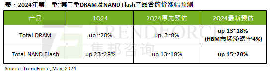 The impact of the AI wave is obvious. TrendForce has revised up its forecast for DRAM memory and NAND flash memory contract price increases this quarter.
May 07, 2024 pm 09:58 PM
The impact of the AI wave is obvious. TrendForce has revised up its forecast for DRAM memory and NAND flash memory contract price increases this quarter.
May 07, 2024 pm 09:58 PM
According to a TrendForce survey report, the AI wave has a significant impact on the DRAM memory and NAND flash memory markets. In this site’s news on May 7, TrendForce said in its latest research report today that the agency has increased the contract price increases for two types of storage products this quarter. Specifically, TrendForce originally estimated that the DRAM memory contract price in the second quarter of 2024 will increase by 3~8%, and now estimates it at 13~18%; in terms of NAND flash memory, the original estimate will increase by 13~18%, and the new estimate is 15%. ~20%, only eMMC/UFS has a lower increase of 10%. ▲Image source TrendForce TrendForce stated that the agency originally expected to continue to
 SK Hynix takes the lead in demonstrating UFS 4.1 universal flash memory, based on V9 TLC NAND particles
Aug 09, 2024 am 10:42 AM
SK Hynix takes the lead in demonstrating UFS 4.1 universal flash memory, based on V9 TLC NAND particles
Aug 09, 2024 am 10:42 AM
According to news from this website on August 9, according to a press release issued by SK Hynix yesterday local time, the company demonstrated a series of new storage products at the FMS2024 Summit, including USF4.1 universal flash memory that has not yet officially released specifications. According to the official website of the JEDEC Solid State Technology Association, the latest UFS specification currently announced is UFS4.0 in August 2022. UFS4.0 specifies a theoretical interface speed of up to 46.4Gbps for each device, and USF4.1 is expected to further improve the transmission rate. ▲JEDECUFS specification page SK Hynix demonstrated two UFS4.1 general-purpose flash memories with capacities of 512GB and 1TB respectively, both based on the 321-layer stacked V91TbTLCNAND flash memory.
 Yangtze Memory QLC flash memory X3-6070 has a write and erase life of 4,000 times, catching up with TLC products
Mar 28, 2024 pm 03:26 PM
Yangtze Memory QLC flash memory X3-6070 has a write and erase life of 4,000 times, catching up with TLC products
Mar 28, 2024 pm 03:26 PM
News from this site on March 28, according to Taiwanese media DIGITIMES, Yangtze Memory stated at the China Flash Memory Market Summit CFMS2024 that the X3-6070QLC flash memory using third-generation Xtacking technology has achieved a P/E endurance of 4,000 times. Note from this site: Different from the warranty life, consumer-grade original TLC solid-state drives generally have at least 3,000 P/E-level erase and write life in tests. ▲Image source China Flash Memory Market Summit CFMS official, the same below Huo Zongliang, CTO of Yangtze Memory, said that the NAND flash memory industry has passed the most difficult year of 2023 and will enter a rising period this year. It is expected that the total flash memory demand will grow at a compound rate from 2023 to 2027. The rate can reach 21%, and the average capacity of a single device is
