 Technology peripherals
 It Industry
 Sources say Intel is considering introducing DSA technology to assist High NA EUV lithography to improve pattern quality
Sources say Intel is considering introducing DSA technology to assist High NA EUV lithography to improve pattern quality
According to news from this site on April 19, foreign media SemiAnalysis and The Elec reported that Intel is considering introducing directional self-assembly DSA technology to assist in future High NA EUV lithography nodes.
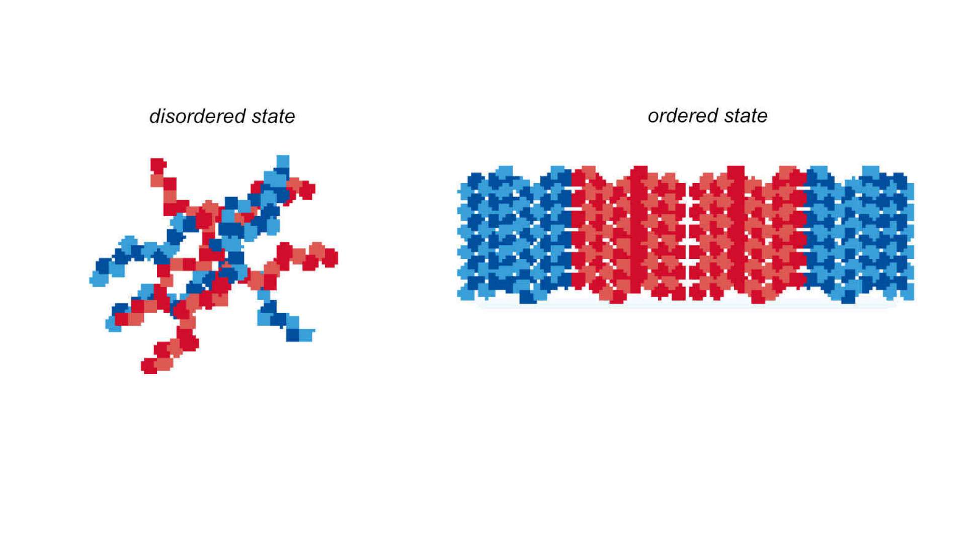
DSA is one of the new patterning technologies that is considered to be able to partially replace traditional photolithography (note on this site: the other is nanoimprinting NIL), which utilizes the molecular properties of chimeric copolymers to achieve Patterning. It is generally considered to be suitable for assisting traditional photolithography rather than being used independently.

SemiAnalysis believes that a big problem facing High NA EUV lithography is the consistency of critical dimensions (CD, a key indicator for measuring the sophistication of semiconductor processes). The contradiction between the timing irradiation dose and the wafer throughput of the photolithography machine leads to the variation of CD. In order to solve this problem, a series of measures need to be taken to improve the stability of the lithography machine and the uniformity of the lithography dose.
If the wafer fab needs to have a good patterning effect while ensuring critical dimensions, then the irradiation dose must be increased. This will slow down the lithography process, reduce the wafer throughput of the lithography machine, and increase the cost burden of the wafer fab.
If the fab runs the lithography machine at a higher throughput, it means that the quality of the lithography pattern decreases as the irradiation dose decreases. At this point, DSA directional self-assembly technology can come into play to repair feature errors on the photolithography pattern.
The introduction ofDSA directional self-assembly can improve the quality of photolithography patterns while reducing the irradiation dose and improving the wafer throughput of the photolithography machine, making High NA EUV lithography more cost-effective sex.
In addition to DSA, Intel is also considering introducing pattern shaping technology into High NA EUV lithography.
Applied Materials released the Centura Sculpta pattern shaping system early last year. This system can precisely modify the characteristic patterns on the wafer in a direction and reduce the number of photolithography times for key layers. It also has the effect of improving the quality of photolithography patterns.
Samsung Electronics also has the intention to introduce the Centura Sculpta system.
Intel researcher Mark Phillip emphasized: "In order to improve the efficiency of the lithography process, it is necessary to introduce equipment other than the lithography machine to supplement it."
The above is the detailed content of Sources say Intel is considering introducing DSA technology to assist High NA EUV lithography to improve pattern quality. For more information, please follow other related articles on the PHP Chinese website!

Hot AI Tools

Undresser.AI Undress
AI-powered app for creating realistic nude photos

AI Clothes Remover
Online AI tool for removing clothes from photos.

Undress AI Tool
Undress images for free

Clothoff.io
AI clothes remover

AI Hentai Generator
Generate AI Hentai for free.

Hot Article

Hot Tools

Notepad++7.3.1
Easy-to-use and free code editor

SublimeText3 Chinese version
Chinese version, very easy to use

Zend Studio 13.0.1
Powerful PHP integrated development environment

Dreamweaver CS6
Visual web development tools

SublimeText3 Mac version
God-level code editing software (SublimeText3)

Hot Topics
 1377
1377
 52
52
 First equipped with Intel Core Ultra 200V series processors, notebooks from ASUS, LG, Dell and MSI are unveiled
Sep 04, 2024 am 07:32 AM
According to news from this site on September 4, Intel officially released the Core Ultra200V series notebook processors at a press conference held in Berlin today. Companies such as ASUS, LG, Dell, and MSI have also launched notebook products equipped with this series of processors. . Overview of the Intel Core Ultra200V series notebook processor launch conference Intel said that the new Lunar Lake processor will provide leading performance and battery life in its class, and it expects that processors of various designs will be on sale later this month. Intel Core Ultra200V Series Notebook Processor Benchmark Demonstration ASUS At this conference, Intel showed off 3 ASUS product prototypes equipped with Core Ultra200V processors: Zenb
 Sources say Samsung Electronics is testing TEL's Acrevia GCB equipment to improve EUV lithography processes
Sep 03, 2024 pm 09:49 PM
According to news from this site on September 3, Korean media TheElec reported yesterday that Samsung is testing Tokyo Electron (TEL)'s AcreviaGCB gas cluster beam (Note from this site: GasClusterBeam) system. TEL's AcreviaGCB system was released on July 8 this year. It can locally and accurately shape EUV lithography patterns through gas cluster beams, thereby repairing pattern defects and reducing pattern roughness. Industry insiders believe that TEL's Acrevia system can play a similar role to Applied Materials' CenturaSculpta system, that is, directly shape EUV exposure patterns, reduce costly EUV multiple exposures, thereby shortening the photolithography process and improving the overall
 What are the top ten virtual currency trading platforms? Ranking of the top ten virtual currency trading platforms in the world
Feb 20, 2025 pm 02:15 PM
With the popularity of cryptocurrencies, virtual currency trading platforms have emerged. The top ten virtual currency trading platforms in the world are ranked as follows according to transaction volume and market share: Binance, Coinbase, FTX, KuCoin, Crypto.com, Kraken, Huobi, Gate.io, Bitfinex, Gemini. These platforms offer a wide range of services, ranging from a wide range of cryptocurrency choices to derivatives trading, suitable for traders of varying levels.
 How to adjust Sesame Open Exchange into Chinese
Mar 04, 2025 pm 11:51 PM
How to adjust Sesame Open Exchange to Chinese? This tutorial covers detailed steps on computers and Android mobile phones, from preliminary preparation to operational processes, and then to solving common problems, helping you easily switch the Sesame Open Exchange interface to Chinese and quickly get started with the trading platform.
 Top 10 virtual currency trading platforms 2025 cryptocurrency trading apps ranking top ten
Mar 17, 2025 pm 05:54 PM
Top Ten Virtual Currency Trading Platforms 2025: 1. OKX, 2. Binance, 3. Gate.io, 4. Kraken, 5. Huobi, 6. Coinbase, 7. KuCoin, 8. Crypto.com, 9. Bitfinex, 10. Gemini. Security, liquidity, handling fees, currency selection, user interface and customer support should be considered when choosing a platform.
 Top 10 cryptocurrency trading platforms, top ten recommended currency trading platform apps
Mar 17, 2025 pm 06:03 PM
The top ten cryptocurrency trading platforms include: 1. OKX, 2. Binance, 3. Gate.io, 4. Kraken, 5. Huobi, 6. Coinbase, 7. KuCoin, 8. Crypto.com, 9. Bitfinex, 10. Gemini. Security, liquidity, handling fees, currency selection, user interface and customer support should be considered when choosing a platform.
 What are the safe and reliable digital currency platforms?
Mar 17, 2025 pm 05:42 PM
A safe and reliable digital currency platform: 1. OKX, 2. Binance, 3. Gate.io, 4. Kraken, 5. Huobi, 6. Coinbase, 7. KuCoin, 8. Crypto.com, 9. Bitfinex, 10. Gemini. Security, liquidity, handling fees, currency selection, user interface and customer support should be considered when choosing a platform.
 Do I need to use flexbox in the center of the Bootstrap picture?
Apr 07, 2025 am 09:06 AM
There are many ways to center Bootstrap pictures, and you don’t have to use Flexbox. If you only need to center horizontally, the text-center class is enough; if you need to center vertically or multiple elements, Flexbox or Grid is more suitable. Flexbox is less compatible and may increase complexity, while Grid is more powerful and has a higher learning cost. When choosing a method, you should weigh the pros and cons and choose the most suitable method according to your needs and preferences.


