
 Technology peripherals
It Industry
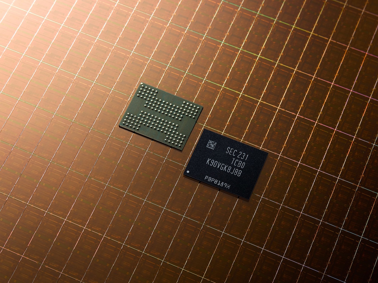
It is reported that Samsung Electronics has basically normalized its NAND flash memory business, with the overall production line utilization reaching 90%.
Technology peripherals
It Industry
It is reported that Samsung Electronics has basically normalized its NAND flash memory business, with the overall production line utilization reaching 90%.
It is reported that Samsung Electronics has basically normalized its NAND flash memory business, with the overall production line utilization reaching 90%.

According to reports from Korean media ETNews, according to industry insiders, Samsung Electronics has recently increased its NAND capacity utilization rate to 90%, a further increase from 80% in the first quarter.
Notes from this site: Regarding Samsung Electronics’ NAND business, Korean media ETNews and The Elec have a relatively optimistic attitude. The latter stated in March that the operating rate of the Xi’an plant has reached 70%; The Chosun Ilbo is even more negative, believing that Samsung continues to maintain its 50% production reduction strategy.
According to reports, Korean electronic media ETNews pointed out that some of Samsung’s large flash memories The storage round plant is actually at full capacity, which is significantly better than the 60% production capacity utilization level in the same period last year.
Reports indicate that the capacity utilization rate of China's Xi'an factory was the first to increase significantly. Since then, the production capacity of Samsung's NAND factory in Pyeongtaek, South Korea, has also been gradually restored.
Another source said that Currently, the NAND flash memory inventory of downstream customers has basically been exhausted, and supply and demand are approaching balance. This is also the confidence for Samsung to continue to increase production capacity utilization.
The report believes that the artificial intelligence boom has driven related companies to increase the demand for enterprise-class solid-state drives, and North American and Chinese cloud service manufacturers have increased their purchases of enterprise-class storage. This is an important factor in the improvement in demand.
The above is the detailed content of It is reported that Samsung Electronics has basically normalized its NAND flash memory business, with the overall production line utilization reaching 90%.. For more information, please follow other related articles on the PHP Chinese website!

Hot AI Tools

Undresser.AI Undress
AI-powered app for creating realistic nude photos

AI Clothes Remover
Online AI tool for removing clothes from photos.

Undress AI Tool
Undress images for free

Clothoff.io
AI clothes remover

AI Hentai Generator
Generate AI Hentai for free.

Hot Article
Hot Tools

Notepad++7.3.1
Easy-to-use and free code editor

SublimeText3 Chinese version
Chinese version, very easy to use

Zend Studio 13.0.1
Powerful PHP integrated development environment

Dreamweaver CS6
Visual web development tools

SublimeText3 Mac version
God-level code editing software (SublimeText3)
Hot Topics
 1379
1379
 52
52

 Fix: Rufus error when formatting on Windows 11
Apr 28, 2023 pm 05:28 PM
Fix: Rufus error when formatting on Windows 11
Apr 28, 2023 pm 05:28 PM
Rufus is an excellent tool for creating bootable installation media, and many people use it to perform a clean installation of Windows on their PC. However, many users have reported Rufus errors on Windows 11. These errors will prevent you from creating installation media, thereby preventing you from installing Windows 11 or any other operating system. Fortunately, fixing these problems is relatively simple, and in today's tutorial, we'll show you the best methods you can use to fix this problem. Why do I get an undetermined error when formatting in Rufus on Windows 11? There are many reasons for this, and in most cases, it's just a software glitch that causes the problem. You can pass
 Commands to install BalenaEtcher on Windows 11
Apr 19, 2023 pm 05:46 PM
Commands to install BalenaEtcher on Windows 11
Apr 19, 2023 pm 05:46 PM
Steps to Install BalenaEtcher on Windows 11 Here we will show the quick way to install BalenaEthcer on Windows 11 without visiting its official website. 1. Open a command terminal (as an administrator), right-click the Start button and select Terminal (Admin). This will open a Windows Terminal with administrative rights to install software and perform other important tasks as superuser. 2. Install BalenaEtcher on Windows 11 Now, on your Windows terminal, just run Using the default Windows package manager
 Industry's highest transfer rate of 3.6GB/s, Micron announces mass production of ninth-generation 276-layer TLC NAND flash memory
Jul 31, 2024 am 08:05 AM
Industry's highest transfer rate of 3.6GB/s, Micron announces mass production of ninth-generation 276-layer TLC NAND flash memory
Jul 31, 2024 am 08:05 AM
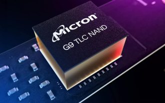
According to news from this site on July 30, Micron announced today (local time) that its ninth generation (site note: 276 layers) 3DTLC NAND flash memory will be mass-produced and shipped. Micron said that its G9NAND has the industry's highest I/O transfer rate of 3.6GB/s (i.e. 3600MT/s flash memory interface rate), which is 50% higher than the existing competing products of 2400MT/s, and can better meet the needs of data-intensive workloads. High throughput requirements. At the same time, Micron's G9NAND is 99% and 88% higher than other solutions on the market in terms of write bandwidth and read bandwidth respectively. This NAND particle-level advantage will bring performance and energy efficiency to solid-state drives and embedded storage solutions. improvement. In addition, like previous generations of Micron NAND flash memory, Micron 276
 Sources say Samsung Electronics and SK Hynix will commercialize stacked mobile memory after 2026
Sep 03, 2024 pm 02:15 PM
Sources say Samsung Electronics and SK Hynix will commercialize stacked mobile memory after 2026
Sep 03, 2024 pm 02:15 PM
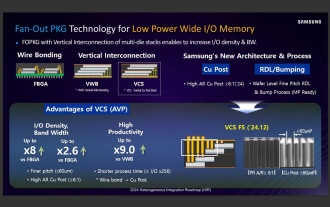
According to news from this website on September 3, Korean media etnews reported yesterday (local time) that Samsung Electronics and SK Hynix’s “HBM-like” stacked structure mobile memory products will be commercialized after 2026. Sources said that the two Korean memory giants regard stacked mobile memory as an important source of future revenue and plan to expand "HBM-like memory" to smartphones, tablets and laptops to provide power for end-side AI. According to previous reports on this site, Samsung Electronics’ product is called LPWide I/O memory, and SK Hynix calls this technology VFO. The two companies have used roughly the same technical route, which is to combine fan-out packaging and vertical channels. Samsung Electronics’ LPWide I/O memory has a bit width of 512
 Samsung announced the completion of 16-layer hybrid bonding stacking process technology verification, which is expected to be widely used in HBM4 memory
Apr 07, 2024 pm 09:19 PM
Samsung announced the completion of 16-layer hybrid bonding stacking process technology verification, which is expected to be widely used in HBM4 memory
Apr 07, 2024 pm 09:19 PM
According to the report, Samsung Electronics executive Dae Woo Kim said that at the 2024 Korean Microelectronics and Packaging Society Annual Meeting, Samsung Electronics will complete the verification of the 16-layer hybrid bonding HBM memory technology. It is reported that this technology has passed technical verification. The report also stated that this technical verification will lay the foundation for the development of the memory market in the next few years. DaeWooKim said that Samsung Electronics has successfully manufactured a 16-layer stacked HBM3 memory based on hybrid bonding technology. The memory sample works normally. In the future, the 16-layer stacked hybrid bonding technology will be used for mass production of HBM4 memory. ▲Image source TheElec, same as below. Compared with the existing bonding process, hybrid bonding does not need to add bumps between DRAM memory layers, but directly connects the upper and lower layers copper to copper.
 Samsung Electronics reiterates that the SF1.4 process is expected to be mass-produced in 2027 and plans to enter the field of co-packaging optics
Jun 13, 2024 pm 05:10 PM
Samsung Electronics reiterates that the SF1.4 process is expected to be mass-produced in 2027 and plans to enter the field of co-packaging optics
Jun 13, 2024 pm 05:10 PM
This site reported on June 13 that Samsung Electronics reiterated at the Samsung Foundry Forum 2024 North America held on June 12, local time, that its SF1.4 process is expected to be mass-produced in 2027, countering previous media rumors. Samsung said its 1.4nm process preparations are progressing smoothly and it is expected to reach mass production milestones in both performance and yield in 2027. In addition, Samsung Electronics is actively researching advanced logic process technology in the post-1.4nm era through innovations in materials and structures to realize Samsung's commitment to continuously surpass Moore's Law. Samsung Electronics simultaneously confirmed that it still plans to mass-produce the second-generation 3nm process SF3 in the second half of 2024. In the more traditional FinFET transistor segment, Samsung Electronics plans to launch S
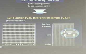
 Samsung's 9th generation V-NAND metal wiring mass production process is revealed to use molybdenum technology for the first time
Jul 03, 2024 pm 05:39 PM
Samsung's 9th generation V-NAND metal wiring mass production process is revealed to use molybdenum technology for the first time
Jul 03, 2024 pm 05:39 PM
According to news from this site on July 3, according to Korean media TheElec, Samsung tried to use molybdenum (Mo) for the first time in the "metal wiring" (metalwiring) of its 9th generation V-NAND. Note from this site: The eight major processes in the semiconductor manufacturing process are: wafer manufacturing oxidation photolithography etching deposition metal wiring testing packaging metal wiring process mainly uses different methods to connect billions of electronic components to form different semiconductors (CPU , GPU, etc.), it can be said to "inject life into semiconductors." Sources say Samsung has introduced five Mo deposition machines from Lam Research, and plans to introduce 20 more pieces of equipment next year. In addition to Samsung Electronics, companies such as SK Hynix, Micron and Kioxia are also
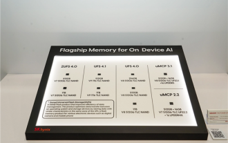 Hynix is the first to demonstrate UFS 4.1 flash memory: based on V9 TLC NAND particles
Aug 09, 2024 pm 03:33 PM
Hynix is the first to demonstrate UFS 4.1 flash memory: based on V9 TLC NAND particles
Aug 09, 2024 pm 03:33 PM
According to news on August 9, at the FMS2024 Summit, SK Hynix demonstrated its latest storage products, including UFS4.1 universal flash memory that has not yet officially released specifications. According to the official website of the JEDEC Solid State Technology Association, the latest UFS specification currently announced is UFS4.0 in August 2022. Its theoretical interface speed is as high as 46.4Gbps. It is expected that UFS4.1 will further improve the transmission rate. 1. Hynix demonstrated 512GB and 1TBUFS4.1 general-purpose flash memory products, based on 321-layer V91TbTLCNAND flash memory. SK Hynix also exhibited 3.2GbpsV92TbQLC and 3.6GbpsV9H1TbTLC particles. Hynix shows off V7-based
