
 Technology peripherals
It Industry
It is reported that Samsung Electronics has established a 1dnm DRAM memory technology development team in advance to rebuild its advantages.
Technology peripherals
It Industry
It is reported that Samsung Electronics has established a 1dnm DRAM memory technology development team in advance to rebuild its advantages.
It is reported that Samsung Electronics has established a 1dnm DRAM memory technology development team in advance to rebuild its advantages.


According to news from this website on May 9, Korean media Sedaily quoted industry sources as saying that Samsung Electronics recently decided to form a technology development team for 1dnm DRAM memory.
The latest process in the DRAM memory industry is the fifth-generation process of the 10 nm series, namely 1bnm;
The next-generation DRAM of the three major memory manufacturers - Samsung Electronics, SK Hynix and Micron The 1cnm process will be put into mass production from the third quarter of this year to next year;
and the 1dnm process is after 1cnm, and the mass production time is expected to be later than 2026.
When Samsung Electronics develops each generation of DRAM process, it generally does not form a comprehensive team including semiconductor and process engineers until the PA (Note of this site: Process Architecture, process architecture) stage close to mass production. The main task of this team is to optimize and adjust process parameters to improve chip performance and reliability. At the same time, they are also responsible for solving various problems and problems encountered during the manufacturing process to ensure that products can be delivered to the market on time.
On the 1dnm node, the team was convened 1 to 2 years earlier, and the current size of the team is around a few hundred people.
Compared with the current process, the 1dnm process will increase the amount of EUV lithography, making it more difficult. Samsung Electronics has established a 1dnm DRAM technology development team in advance to accelerate mass production preparations and shorten the process optimization cycle.
Since 2020, Samsung Electronics has struggled to maintain its lead in DRAM memory technology:
At the 1anm node, Micron took the lead in mass production; when it came to 1bnm, the three companies took the lead in mass production Roughly the same; and in the upcoming 1cnm node, SK Hynix is expected to take the lead.
On the product side, due to the previous wrong decision to disband the HBM memory R&D team, Samsung Electronics is currently lagging behind in the competition of HBM3 (E) memory.
Samsung Electronics hopes to stop the current decline by increasing human resource investment in 1dnm DRAM development in advance, re-establish its memory technology advantages, and promote HBM business development through DRAM technology upgrades.
The above is the detailed content of It is reported that Samsung Electronics has established a 1dnm DRAM memory technology development team in advance to rebuild its advantages.. For more information, please follow other related articles on the PHP Chinese website!

Hot AI Tools

Undresser.AI Undress
AI-powered app for creating realistic nude photos

AI Clothes Remover
Online AI tool for removing clothes from photos.

Undress AI Tool
Undress images for free

Clothoff.io
AI clothes remover

AI Hentai Generator
Generate AI Hentai for free.

Hot Article
Hot Tools

Notepad++7.3.1
Easy-to-use and free code editor

SublimeText3 Chinese version
Chinese version, very easy to use

Zend Studio 13.0.1
Powerful PHP integrated development environment

Dreamweaver CS6
Visual web development tools

SublimeText3 Mac version
God-level code editing software (SublimeText3)
Hot Topics
 1376
1376
 52
52

 Large memory optimization, what should I do if the computer upgrades to 16g/32g memory speed and there is no change?
Jun 18, 2024 pm 06:51 PM
Large memory optimization, what should I do if the computer upgrades to 16g/32g memory speed and there is no change?
Jun 18, 2024 pm 06:51 PM
For mechanical hard drives or SATA solid-state drives, you will feel the increase in software running speed. If it is an NVME hard drive, you may not feel it. 1. Import the registry into the desktop and create a new text document, copy and paste the following content, save it as 1.reg, then right-click to merge and restart the computer. WindowsRegistryEditorVersion5.00[HKEY_LOCAL_MACHINE\SYSTEM\CurrentControlSet\Control\SessionManager\MemoryManagement]"DisablePagingExecutive"=d
 Sources say SK Hynix's five-layer stacked 3D DRAM memory yield has reached 56.1%
Jun 24, 2024 pm 01:52 PM
Sources say SK Hynix's five-layer stacked 3D DRAM memory yield has reached 56.1%
Jun 24, 2024 pm 01:52 PM
According to news from this website on June 24, Korean media BusinessKorea reported that industry insiders revealed that SK Hynix published the latest research paper on 3D DRAM technology at the VLSI 2024 Summit held in Hawaii, USA from June 16 to 20. In this paper, SK Hynix reports that its five-layer stacked 3D DRAM memory yield has reached 56.1%, and the 3D DRAM in the experiment exhibits similar characteristics to current 2D DRAM. According to reports, unlike traditional DRAM, which arranges memory cells horizontally, 3D DRAM stacks cells vertically to achieve higher density in the same space. However, SK hynix
 How to check memory usage on Xiaomi Mi 14Pro?
Mar 18, 2024 pm 02:19 PM
How to check memory usage on Xiaomi Mi 14Pro?
Mar 18, 2024 pm 02:19 PM
Recently, Xiaomi released a powerful high-end smartphone Xiaomi 14Pro, which not only has a stylish design, but also has internal and external black technology. The phone has top performance and excellent multitasking capabilities, allowing users to enjoy a fast and smooth mobile phone experience. However, performance will also be affected by memory. Many users want to know how to check the memory usage of Xiaomi 14Pro, so let’s take a look. How to check memory usage on Xiaomi Mi 14Pro? Introduction to how to check the memory usage of Xiaomi 14Pro. Open the [Application Management] button in [Settings] of Xiaomi 14Pro phone. To view the list of all installed apps, browse the list and find the app you want to view, click on it to enter the app details page. In the application details page
 Is there a big difference between 8g and 16g memory in computers? (Choose 8g or 16g of computer memory)
Mar 13, 2024 pm 06:10 PM
Is there a big difference between 8g and 16g memory in computers? (Choose 8g or 16g of computer memory)
Mar 13, 2024 pm 06:10 PM
When novice users buy a computer, they will be curious about the difference between 8g and 16g computer memory? Should I choose 8g or 16g? In response to this problem, today the editor will explain it to you in detail. Is there a big difference between 8g and 16g of computer memory? 1. For ordinary families or ordinary work, 8G running memory can meet the requirements, so there is not much difference between 8g and 16g during use. 2. When used by game enthusiasts, currently large-scale games basically start at 6g, and 8g is the minimum standard. Currently, when the screen is 2k, higher resolution will not bring higher frame rate performance, so there is no big difference between 8g and 16g. 3. For audio and video editing users, there will be obvious differences between 8g and 16g.
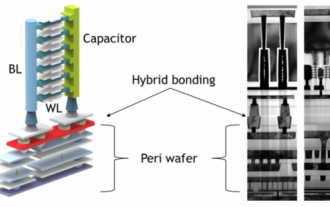
 Samsung announced the completion of 16-layer hybrid bonding stacking process technology verification, which is expected to be widely used in HBM4 memory
Apr 07, 2024 pm 09:19 PM
Samsung announced the completion of 16-layer hybrid bonding stacking process technology verification, which is expected to be widely used in HBM4 memory
Apr 07, 2024 pm 09:19 PM
According to the report, Samsung Electronics executive Dae Woo Kim said that at the 2024 Korean Microelectronics and Packaging Society Annual Meeting, Samsung Electronics will complete the verification of the 16-layer hybrid bonding HBM memory technology. It is reported that this technology has passed technical verification. The report also stated that this technical verification will lay the foundation for the development of the memory market in the next few years. DaeWooKim said that Samsung Electronics has successfully manufactured a 16-layer stacked HBM3 memory based on hybrid bonding technology. The memory sample works normally. In the future, the 16-layer stacked hybrid bonding technology will be used for mass production of HBM4 memory. ▲Image source TheElec, same as below. Compared with the existing bonding process, hybrid bonding does not need to add bumps between DRAM memory layers, but directly connects the upper and lower layers copper to copper.
 Sources say Samsung Electronics and SK Hynix will commercialize stacked mobile memory after 2026
Sep 03, 2024 pm 02:15 PM
Sources say Samsung Electronics and SK Hynix will commercialize stacked mobile memory after 2026
Sep 03, 2024 pm 02:15 PM
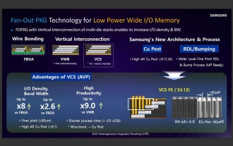
According to news from this website on September 3, Korean media etnews reported yesterday (local time) that Samsung Electronics and SK Hynix’s “HBM-like” stacked structure mobile memory products will be commercialized after 2026. Sources said that the two Korean memory giants regard stacked mobile memory as an important source of future revenue and plan to expand "HBM-like memory" to smartphones, tablets and laptops to provide power for end-side AI. According to previous reports on this site, Samsung Electronics’ product is called LPWide I/O memory, and SK Hynix calls this technology VFO. The two companies have used roughly the same technical route, which is to combine fan-out packaging and vertical channels. Samsung Electronics’ LPWide I/O memory has a bit width of 512
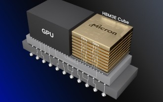 Micron: HBM memory consumes 3 times the wafer volume, and production capacity is basically booked for next year
Mar 22, 2024 pm 08:16 PM
Micron: HBM memory consumes 3 times the wafer volume, and production capacity is basically booked for next year
Mar 22, 2024 pm 08:16 PM
This site reported on March 21 that Micron held a conference call after releasing its quarterly financial report. At the conference, Micron CEO Sanjay Mehrotra said that compared to traditional memory, HBM consumes significantly more wafers. Micron said that when producing the same capacity at the same node, the current most advanced HBM3E memory consumes three times more wafers than standard DDR5, and it is expected that as performance improves and packaging complexity intensifies, in the future HBM4 This ratio will further increase. Referring to previous reports on this site, this high ratio is partly due to HBM’s low yield rate. HBM memory is stacked with multi-layer DRAM memory TSV connections. A problem with one layer means that the entire
 Samsung Electronics reiterates that the SF1.4 process is expected to be mass-produced in 2027 and plans to enter the field of co-packaging optics
Jun 13, 2024 pm 05:10 PM
Samsung Electronics reiterates that the SF1.4 process is expected to be mass-produced in 2027 and plans to enter the field of co-packaging optics
Jun 13, 2024 pm 05:10 PM
This site reported on June 13 that Samsung Electronics reiterated at the Samsung Foundry Forum 2024 North America held on June 12, local time, that its SF1.4 process is expected to be mass-produced in 2027, countering previous media rumors. Samsung said its 1.4nm process preparations are progressing smoothly and it is expected to reach mass production milestones in both performance and yield in 2027. In addition, Samsung Electronics is actively researching advanced logic process technology in the post-1.4nm era through innovations in materials and structures to realize Samsung's commitment to continuously surpass Moore's Law. Samsung Electronics simultaneously confirmed that it still plans to mass-produce the second-generation 3nm process SF3 in the second half of 2024. In the more traditional FinFET transistor segment, Samsung Electronics plans to launch S
